onsemi FGH75N60UF
This Device is Pb−Free and is RoHS Compliant Applications • Solar Inverters, UPS, Welder, PFC VCES 600 V IC 75 A C G E E C G COLLECTOR (FLANGE) TO−247−3LD CASE 340CK MARKING DIAGRAM $Y&Z&3&K FGH75N60 UF © Semiconductor Components Industries, LLC, 2008 March, 2020 − Rev. for Soldering Purposes, 1/8” from Case for 5 Seconds 300 °C Stresses exceeding those listed in the Maximum Ratings table may damage the device.| Part No. | FGH75N60UF |
|---|---|
| Datasheet | FGH75N60UF Download |
| Manufacturer |  onsemi |
| Description | IGBT |
| Buy | Stock & Price |

DESCRIPTION
Using novel field stop IGBT technology, ON Semiconductor’s field stop IGBTs offer the optimum performance for solar inverter, UPS, welder and PFC applications where low conduction and switching losses are essential.FEATURES
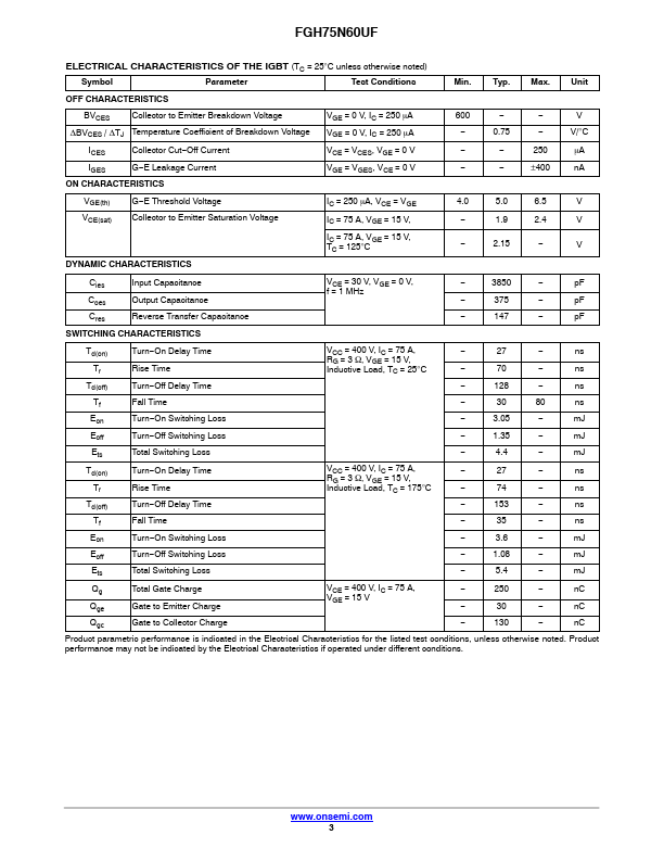
● High Current Capability● Low Saturation Voltage: VCE(sat) = 1.9 V (Typ.) @ IC = 75 A
● High Input Impedance
● Fast Switching
● 2 $Y &Z &3 &K FGH75N60UF = ON Semiconductor Logo = Assembly Plant Code = Numeric Date Code = Lot Code = Specific Device Code ORDERING INFORMATION See detailed ordering and shipping information on page 2 of this data sheet. 1 Publication Order Number: FGH75N60UF/D FGH75N60UF
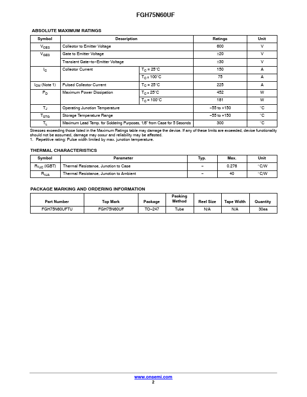
ABSOLUTE MAXIMUM RATINGS
SymbolDESCRIPTION
Ratings Unit VCES VGES Collector to Emitter Voltage Gate to Emitter Voltage Transient Gate−to−Emitter Voltage 600 V ±20 V ±30 V IC Collector Current TC = 25°C 150 A TC = 100°C 75 A ICM (Note 1) Pulsed Collector Current TC = 25°C 225 A PD Maximum Power Dissipation TC = 25°C 452 W TC = 100°C 181 W TJ Operating Junction Temperature −55 to +150 °C TSTG Storage Temperature Range −55 to +150 °C TL Maximum Lead Temp.