onsemi NSVJ3557SA3
N-Channel JFET
| Part No. | NSVJ3557SA3 |
|---|---|
| Datasheet | NSVJ3557SA3 Download |
| Manufacturer |  onsemi |
| Description | N-Channel JFET |
| Buy | Stock & Price |
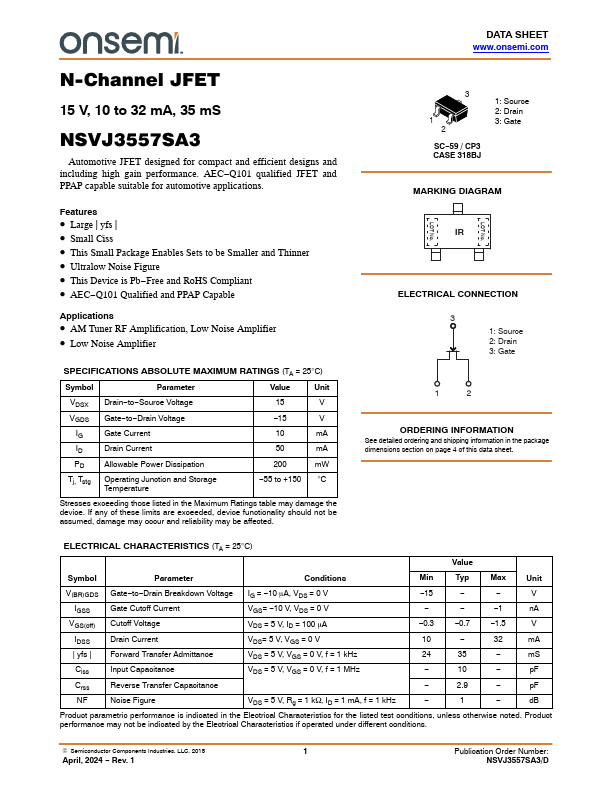
FEATURES
● Large | yfs |● Small Ciss
● This Small Package Enables Sets to be Smaller and Thinner
● Ultralow Noise Figure
● This Device is Pb−Free and RoHS Compliant
● AEC−Q101 Qualified and PPAP Capable
APPLICATIONS
● AM Tuner RF Amplification, Low Noise Amplifier● Low Noise Amplifier SPECIFICATIONS
ABSOLUTE MAXIMUM RATINGS
(TA = 25°C) Symbol Parameter Value Unit VDSX Drain−to−Source Voltage 15 V VGDS IG ID PD Tj, Tstg Gate−to−Drain Voltage Gate Current Drain Current Allowable Power Dissipation Operating Junction and Storage Temperature −15 V 10 mA 50 mA 200 mW −55 to +150 °C Stresses exceeding those listed in theMAXIMUM RATINGS
table may damage the device. If any of these limits are exceeded, device functionality should not be assumed, damage may occur and reliability may be affected. 3 1 2 SC−59 / CP3 CASE 318BJ 1: Source 2: Drain 3: Gate MARKING DIAGRAM IR LOT No. LOT No. ELECTRICAL CONNECTION 3 1: Source 2: Drain 3: Gate 1 2 ORDERING INFORMATION See detailed ordering and shipping information in the package dimensions section on page 4 of this data sheet.