onsemi NVJD4152P
Dual P-Channel MOSFET
| Part No. | NVJD4152P |
|---|---|
| Datasheet | NVJD4152P Download |
| Manufacturer |  onsemi |
| Description | Dual P-Channel MOSFET |
| Buy | Stock & Price |

FEATURES
● Leading Trench Technology for Low RDS(ON) Performance● Small Footprint Package (SC70−6 Equivalent)
● ESD Protected Gate
● NV Prefix for Automotive and Other
APPLICATIONS
Requiring Unique Site and Control Change Requirements; AEC−Q101 Qualified and PPAP Capable● These are Pb−Free Devices
APPLICATIONS
● Load/Power Management● Charging Circuits
● Load Switching
● Cell Phones, Computing, Digital Cameras, MP3s and PDAs
MAXIMUM RATINGS
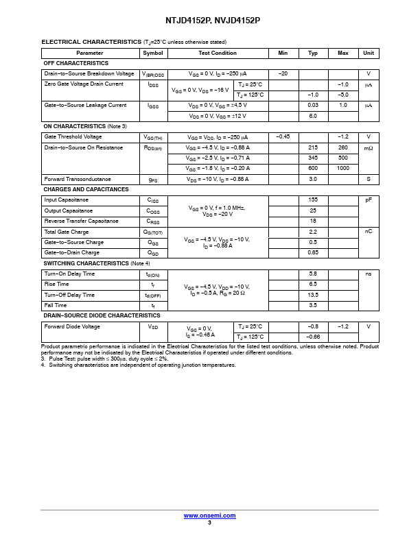
(TJ = 25°C unless otherwise stated) Parameter Symbol Value Unit Drain−to−Source Voltage VDSS −20 V Gate−to−Source Voltage VGS ±12 V Continuous Drain Current (Note 1) Steady TA = 25°C ID State TA = 85°C −0.88 A −0.63 Power Dissipation (Note 1) Steady TA = 25°C PD State TA = 85°C 0.272 W 0.141 Continuous Drain Current (Note 2) t v 5 s TA = 25°C ID TA = 85°C −1.0 A −0.72 Power Dissipation (Note 2) t v 5 s TA = 25°C PD TA = 85°C 0.35 W 0.181 Pulsed Drain Current t ≤ 10 ms IDM ±3.0 A Operating Junction and Storage Temperature TJ, −55 to °C TSTG 150 Co...