Description
10
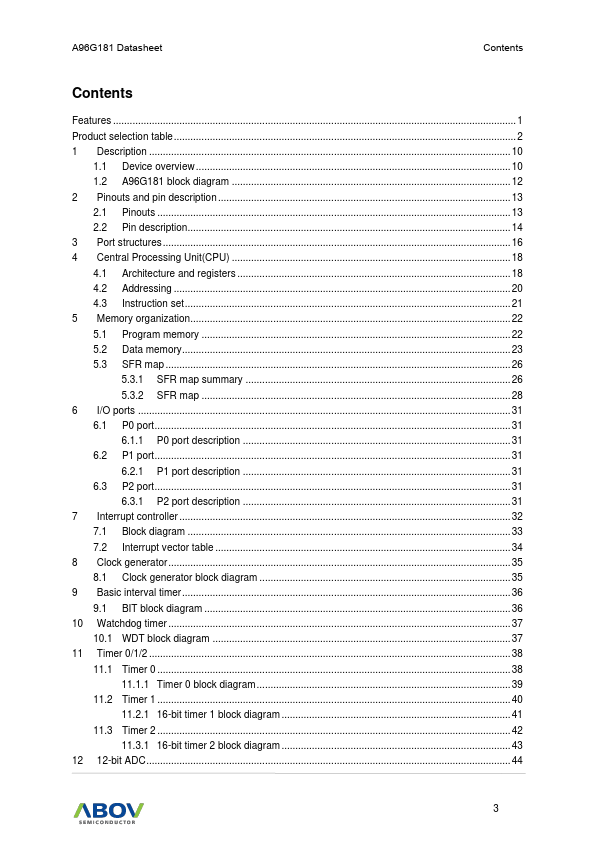
1.1 Device overview 10 1.2 A96G181 block diagram 12 2 Pinouts and pin description 13 2.1 Pinouts 13 2.2 Pin description 14 3 Port structures 16 4 Central Processing Unit(CPU) 18 4.1 Architecture and registers 18 4.2 Addressing 20 4.3 Instruction set 21 5 Memory organization 22 5.1 Program memory 22 5.2 Data memory 23 5.3 SFR map 26
5.3.1 SFR map summary 26 5.3.2 SFR map 28 6 I/O ports
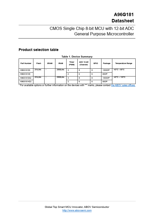
Features
- Core.
- 8-bit CISC M8051 core (8051 Compatible, 2 clocks per cycle)
2 Kbytes On-Chip FLASH.
- Endurance : 30,000 times.
- In-System Programming (ISP).
- Retention : 10 years
256 bytes IRAM
General Purpose I/O (GPIO).
- Normal I/O : 8 ports ( P0[3:0], P1[7:6], P2[1:0] )
Timer/Counter.
- Basic Interval Timer (BIT) 8-bit × 1-ch.
- Watch Dog Timer (WDT) 8-bit × 1-ch.
- 8-bit × 1-ch (T0).
- 16-bit × 2-ch (T1/T2)
Programmable Pulse Generation.
- 16-bit Pulse generation (b.
 A96G181-ABOV.pdf