Description
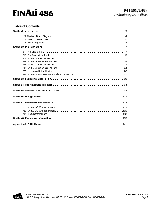
1.3 Block Diagrams 4
Section 2: Pin Description 7
2.1 Pin Diagrams 7 2.2 Pin Description Table 9 2.3 M1489 Numerical Pin List 17 2.4 M1489 Alphabetical Pin List 19 2.5 M1487 Numerical Pin List 22 2.6 M1487 Alphabetical Pin List 24 2.7 Hardware Setup Control 26 2.8 M1489/M1487 Hardware Reference Manual 27
Section 3: Functional Description 30 Section 4: Configuration Registers 34 Section 5: Software Programming Guide 94 Section 6: Design Issues107 Section 7: Electrical Characteristics 133
7.1 M14
Features
- M1489 (Cache-Memory PCI controller) M1487 (ISA Bus Controller)
Supported CPUs T Supports AMD 486D4 and X5, Intel 486, P24T, P24D,
DX4, SL-Enhanced, Cyrix M7, UMC U5 and AMD AM486DXL CPUs in 25, 33, 40, 50, 66, 100 and 133 MHz 3V/5V CPU interface
T Supports CPU L1 writeback T Supports Cyrix's linear addressing mode
L2 Cache Controller T Write Back cache with standard SRAM T 8 Tag Bits, always force Dirty or
7 Tag Bits, 1 Dirty bit
T Supports cache size of 128K to 1M with 32Kx8,
64Kx8, 128Kx8
T Su.


