AD7452
AD7452 is 12-Bit ADC manufactured by Analog Devices.
FEATURES
Specified for VDD of 3 V and 5 V Low power at max throughput rate: 3.3 m W max at 555 k SPS with 3 V supplies 7.25 m W max at 555 k SPS with 5 V supplies Fully differential analog input Wide input bandwidth: 70 d B SINAD at 100 k Hz input frequency Flexible power/serial clock speed management No pipeline delays High speed serial interface: SPI®/QSPI™/MICROWIRE™/DSP patible Power-down mode: 1 µA max 8-lead SOT-23 package
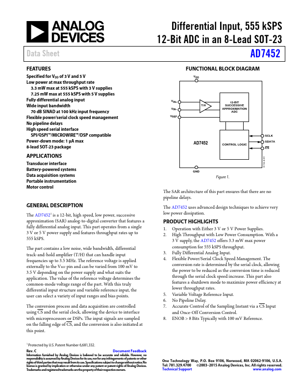
FUNCTIONAL BLOCK DIAGRAM
VIN+ T/H VIN- VREF
12-BIT SUCCESSIVE APPROXIMATION ADC
SCLK
SDATA CONTROL LOGIC CS
03154-A-001
APPLICATIONS
Transducer interface Battery-powered systems Data acquisition systems Portable instrumentation Motor control
Figure 1.
GENERAL DESCRIPTION
The AD74521 is a 12-bit, high speed, low power, successive approximation (SAR) analog-to-digital converter that features a fully differential analog input. This part operates from a single 3 V or 5 V power supply and features throughput rates up to 555 k SPS. The part contains a low noise, wide bandwidth, differential track-and-hold amplifier (T/H) that can handle input frequencies up to 3.5 MHz. The reference voltage is applied externally to the VREF pin and can be varied from 100 m V to 3.5 V depending on the power supply and what suits the application. The value of the reference voltage determines the mon-mode voltage range of the part. With this truly differential input structure and variable reference input, the user can select a variety of input ranges and bias points. The conversion process and data acquisition are controlled using CS and the serial clock, allowing the device to interface with microprocessors or DSPs. The input signals are sampled on the falling edge of CS, and the conversion is also initiated at this point.
The SAR architecture of this part ensures that there are no pipeline delays. The AD7452 uses advanced design techniques to achieve very low power dissipation.
PRODUCT HIGHLIGHTS
1. 2. Operation with Either 3 V or 5 V Power...