Datasheet Details
| Part number | ADN2865 |
|---|---|
| Manufacturer | Analog Devices |
| File Size | 476.54 KB |
| Description | Clock and Data Recovery |
| Datasheet |
 ADN2865_AnalogDevices.pdf ADN2865_AnalogDevices.pdf
|
|
|
The ADN2865 by Analog Devices is a Clock and Data Recovery. Below is the official datasheet preview.
| Part number | ADN2865 |
|---|---|
| Manufacturer | Analog Devices |
| File Size | 476.54 KB |
| Description | Clock and Data Recovery |
| Datasheet |
ADN2865_AnalogDevices.pdf
|
|
|
|
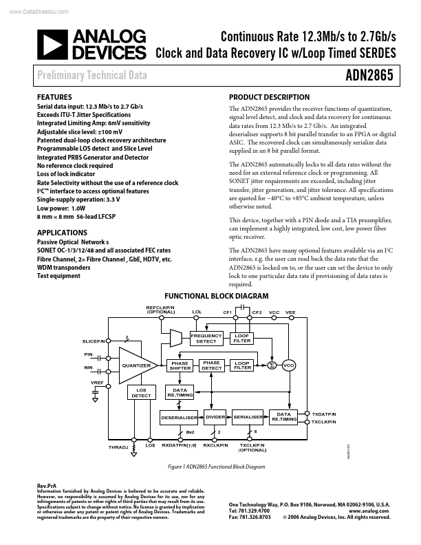
The ADN2865 provides the receiver functions of quantization, signal level detect, and clock and data recovery for continuous data rates from 12.3 Mb/s to 2.7 Gb/s.
📁 ADN2865 Similar Datasheet