Datasheet4U Logo Datasheet4U.com

ADN4666

Quad CMOS Differential Line Receiver

ADN4666 Features

* ±8 kV ESD IEC 61000-4-2 contact discharge on receiver input pins 400 Mbps (200 MHz) switching rates 100 ps channel-to-channel skew (typical) 100 ps differential skew (typical) 3.3 ns propagation delay (maximum) 3.3 V power supply High impedance outputs on power-down Low power design (10 mW quiescent

ADN4666 General Description

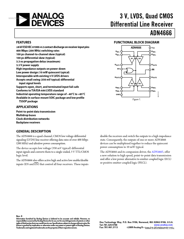
The ADN4666 is a quad-channel, CMOS low voltage differential signaling (LVDS) line receiver offering data rates of over 400 Mbps (200 MHz) and ultralow power consumption. The device accepts low voltage (350 mV typical) differential input signals and converts them to a single-ended, 3 V TTL/CMOS logi.

ADN4666 Datasheet (371.64 KB)

Preview of ADN4666 PDF

Datasheet Details

Part number:

ADN4666

Manufacturer:

Analog Devices ↗

File Size:

371.64 KB

Description:

Quad cmos differential line receiver.
www.DataSheet4U.com 3 V, LVDS, Quad CMOS Differential Line Receiver ADN4666 FUNCTIONAL BLOCK DIAGRAM ADN4666 RIN1

* RIN1+ R1 ROUT1 EN R4 ROUT4.

📁 Related Datasheet

ADN4661 - High Speed Differential Driver (Analog Devices)
.. Single, 3 V, CMOS, LVDS, High Speed Differential Driver ADN4661 FUNCTIONAL BLOCK DIAGRAM VCC FEATURES ±15 kV ESD protection on o.

ADN4662 - LVDS Differential Line Receiver (Analog Devices)
.. Single, 3 V, CMOS, LVDS Differential Line Receiver ADN4662 FUNCTIONAL BLOCK DIAGRAM VCC FEATURES ±15 kV ESD protection on input .

ADN4663 - LVDS High Speed Differential Driver (Analog Devices)
FEATURES ±15 kV ESD protection on output pins 600 Mbps (300 MHz) switching rates Flow-through pinout simplifies PCB layout 300 ps typical differential.

ADN4664 - LVDS Differential Line Receiver (Analog Devices)
.. Dual, 3 V, CMOS, LVDS Differential Line Receiver ADN4664 FUNCTIONAL BLOCK DIAGRAM VCC FEATURES ±15 kV ESD protection on output p.

ADN4665 - CMOS Differential Line Driver (Analog Devices)
.. 3 V, LVDS, Quad, CMOS Differential Line Driver ADN4665 FUNCTIONAL BLOCK DIAGRAM ADN4665 DIN1 D1 DOUT1+ DOUT1– EN D4 DOUT4+ DOUT4–.

ADN4667 - 3V LVDS Quad CMOS Differential Line Driver (Analog Devices)
.. 3 V LVDS Quad CMOS Differential Line Driver ADN4667 FUNCTIONAL BLOCK DIAGRAM VCC FEATURES ±15 kV ESD protection on output pins 4.

ADN4668 - 3V LVDS Quad CMOS Differential Line Receiver (Analog Devices)
.. 3 V LVDS Quad CMOS Differential Line Receiver ADN4668 FUNCTIONAL BLOCK DIAGRAM VCC FEATURES ±15 kV ESD protection on receiver in.

ADN4600 - Asynchronous Crosspoint Switch (Analog Devices)
.. 4.25 Gbps, 8 × 8, Asynchronous Crosspoint Switch ADN4600 FUNCTIONAL BLOCK DIAGRAM ADN4600 RECEIVE EQUALIZATION IP[7:0] EQ IN[7:0].

TAGS

ADN4666 Quad CMOS Differential Line Receiver Analog Devices

Image Gallery

ADN4666 Datasheet Preview Page 2 ADN4666 Datasheet Preview Page 3

ADN4666 Distributor