APM4953
Features
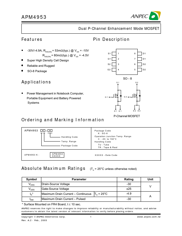
Pin Description
- -30V/-4.9A, RDS(ON) = 53mΩ(typ.) @ VGS = -10V
RDS(ON) = 80mΩ(typ.) @ VGS = -4.5V
- Super High Density Cell Design
- Reliable and Rugged
- SO-8 Package
Applications
5 / 5! /"
& , % , $, #,
- 8
5 5
- Power Management in Notebook puter,
Portable Equipment and Battery Powered Systems
/ /
Ordering and Marking Information
, ,
,,
P-Channel MOSFET
APM4953 K :
H andling C ode Temp. Range Package Code
A P M 4953 XXXXX
Package Code K : SO -8
O peration Junction Tem p. R ange C : -55 to 150°C
H andling C ode TU : Tube TR : Tape & Reel
XXXXX
- Date Code
Absolute Maximum Ratings (TA = 25°C unless otherwise noted)
Symbol
Parameter
Rating
Unit
VDSS VGSS ID- IDM
Drain-Source Voltage Gate-Source Voltage Maximum Drain Current Continuous TA = 25°C Maximum Drain Current Pulsed
-30 V
±25 -4.9
A -30
- Surface Mounted on FR4 Board, t ≤ 10 sec.
ANPEC reserves the right to make changes to improve reliability or manufacturability...