C460UT190
C460UT190 is LED manufactured by Cree.
FEATURES
- Wavelengths for Blue, Green and White-conversion
- 50 mm Chip Thickness
- RF Performance:
- 450 nm
- 12+ m W
- 460 nm
- 10+ m W
- 470 nm
- 10+ m W
- 527 nm
- 4+ m W
- Low Forward Voltage
- 2.9 V Typical at 5 m A
- Conductive Adhesive Die Attach
- Single Wire Bond, Vertically Conductive Structure
- 2k V Class 2 ESD Rating
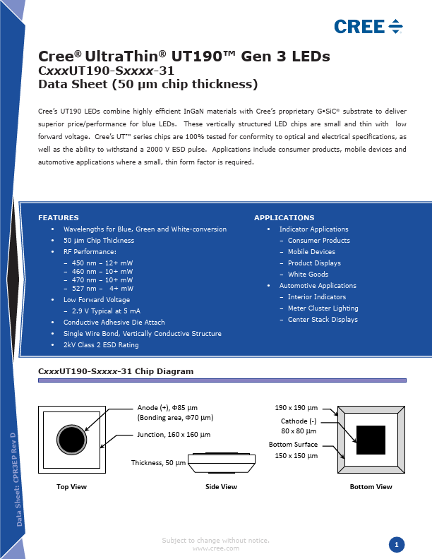
Cxxx UT190-Sxxxx-31 Chip Diagram
APPLICATIONS
- Indicator Applications
- Consumer Products
- Mobile Devices
- Product Displays
- White Goods
- Automotive Applications
- Interior Indicators
- Meter Cluster Lighting
- Center Stack Displays
Top View
Anode (+), Ф85 mm (Bonding area, Ф70 mm) Junction, 160 x 160 mm
Thickness, 50 mm
Side View
190 x 190 mm
Cathode (-) 80 x 80 mm
Bottom Surface 150 x 150 mm
Bottom View
Subject to change without notice. .cree.
Data Sheet: CPR3EP Rev D
Maximum Ratings at TA = 25°C Notes 1&3 DC Forward Current Peak Forward Current (1/10 duty cycle @ 1 k Hz) LED Junction Temperature Reverse Voltage Operating Temperature Range LED Chip Storage Temperature Range (LED Chip only, not for Die Sheet Storage) Remended Die Sheet Storage Conditions Electrostatic Discharge Threshold (HBM) Note 2 Electrostatic Discharge Classification (MIL-STD-883E) Note...