CW24C04
DESCRIPTION
The CW24C02/04/08/16 is Electrically Erasable PROM. The device is organized as one block of 256/512/1024/2048 x 8-bit memory with 2-wire serial interface. Low-voltage design permits operation down to 1.8V, with standby and active currents of only 1μA and 1m A respectively. The CW24C02/04/08/16 also has a page write capability for up to 8/16/16/16 bytes of data.
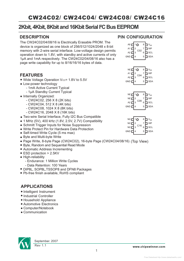
PIN CONFIGURATION
A0 A1 A2 GND 1 2 3 4 8 VCC WP SCL SDA
C02
7 6 5
1 2 3
VCC WP SCL
FEATURES
A1 A2
C04
7 6
- Wide Voltage Operation VCC= 1.8V to 5.5V GND 5 4 SDA
- Low-power technology
- 1m A Active Current Typical
- 1μA Standby Current Typical VCC NC 8 1
- Internally Organized: WP NC 7 2
- CW24C02, 256 X 8 (2K bits) C08 SCL A2 6 3
- CW24C04, 512 X 8 (4K bits) SDA GND 5 4
- CW24C08, 1024 X 8 (8K bits)
- CW24C16, 2048 X 8 (16K bits)
- Two-wire Serial Interface, Fully I2C Bus patible NC 8 VCC 1
- 1 MHz (5V), 400 k Hz (1.8V, 2.5V, 2.7V) patibility NC 7 WP 2
- Schmitt Trigger Inputs for Noise Suppression...