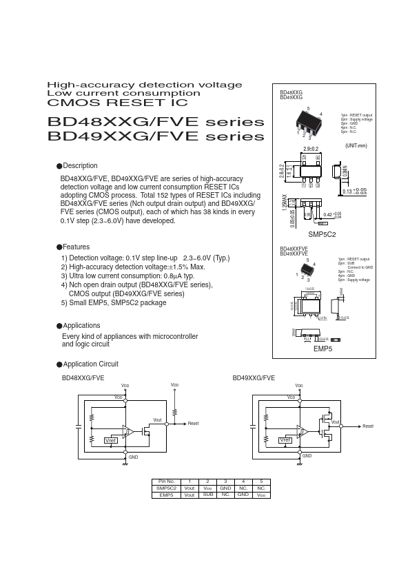
Description
Reset
Vref
Vref
GND
GND
Pin No.SMP5C2 EMP5
1 Vout Vout
2 VDD SUB
3 GND NC.4 NC.GND
5 NC.VDD
http://www.Datasheet4U.com
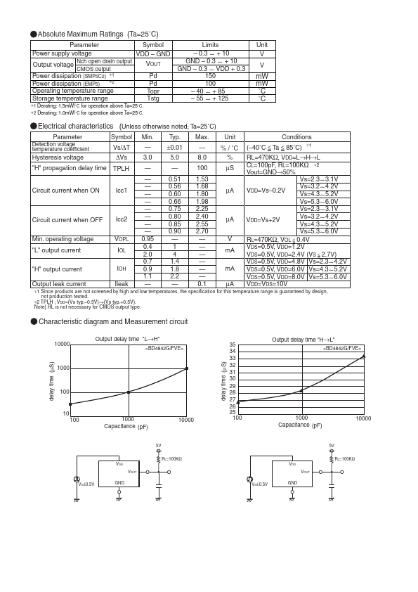
Absolute Maximum Ratings (Ta=25˚C)
Parameter Power supply voltage
CMOS output Power dissipation (SMP5C2) ∗1 Power dissipation (EMP5) ∗2
Symbol VDD
GND VOUT Pd Pd Topr Tstg
Output voltage Nch open drain output
Operating temperature range Storage temperature range
Limits
0.3 ~ + 10 GND
0.3 ~ + 10 GND
0.3 ~ VDD + 0.3 150
Features
- 1) Detection voltage: 0.1V step line-up 2.3~6.0V (Typ. ) 2) High-accuracy detection voltage:±1.5% Max. 3) Ultra low current consumption: 0.8µA typ. 4) Nch open drain output (BD48XXG/FVE series), CMOS output (BD49XXG/FVE series) 5) Small EMP5, SMP5C2 package.
 BD4860G-ETC.pdf