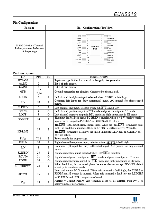
Description
PIN PIN I/O DESCRIPTION
BYPASS GAIN0 GAIN1 GND LHPIN LIN LLINEIN LOUT+ LOUTPC-BEEP
11 2 3 1,12 13,24 6 10 5 4 9 14
I I
Tap to voltage divider for internal mid-supply bias generator Bit 0 of gain control Bit 1 of gain control Ground connection for circuitry.Connected to thermal pad.I I I O O I
HP/ LINE
PVDD RHPIN RIN RLINEIN ROUT+ ROUT-
17 7,18 20 8 23 21 16
I I I I I O O
SHUTDOWN SE/ BTL VDD
22 15 19
I I I
Left channel headphone input, selected when SE/ BTL is held high.Common lef
Features
 EUA5312_EutechMicroelectronics.pdf