Description
1 2
3
4
5
6
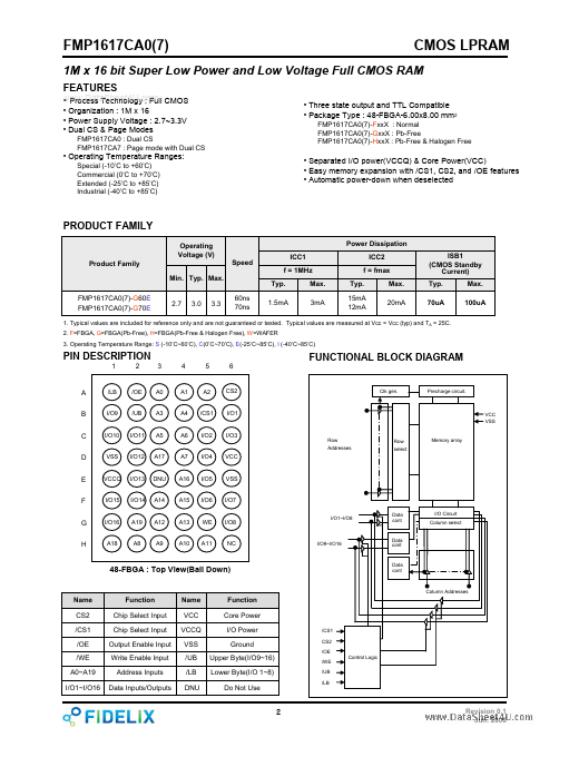
FUNCTIONAL BLOCK DIAGRAM
Precharge circuit.A B C D E F G H
/LB I/O9
/OE /UB
A0 A3
A1 A4
A2 /CS1
CS2 I/O1
Clk gen.VCC VSS Memory array
I/O10 VSS
I/O11 I/O12
A5 A17
A6 A7 A16
I/O2 I/O4 I/O5
I/O3 VCC VSS
Row Addresses
Row select
VCCQ I/O15 I/O16 A18
I/O13 I/O14 A19 A8
DNU A14 A12 A9
A15 A13 A10
I/O6
I/O7 I/O8
I/O1~I/O8 Data cont I/O Circuit Column select
WE A11
NC
I/O9~I/O16
Data cont
48-FBGA : Top View(Ball Down)
Data cont
Column Addresses
Name CS2
Features
- www. DataSheet4U. com.
- Process Technology : Full CMOS.
- Organization : 1M x 16.
- Power Supply Voltage : 2.7~3.3V.
- Dual CS & Page Modes
FMP1617CA0 : Dual CS FMP1617CA7 : Page mode with Dual CS
CMOS LPRAM
1M x 16 bit Super Low Power and Low Voltage Full CMOS RAM.
- Three state output and TTL Compatible.
- Package Type : 48-FBGA-6.00x8.00 mm2
FMP1617CA0(7)-FxxX : Normal FMP1617CA0(7)-GxxX : Pb-Free FMP1617CA0(7)-HxxX : Pb-Free & Halogen Free.
 FMP1617CA0_FIDELIX.pdf