FDD86326
Features
General Description
- Shielded Gate MOSFET Technology
- Max r DS(on) = 23 mΩ at VGS = 10 V, ID = 8 A
- Max r DS(on) = 37 mΩ at VGS = 6 V, ID = 4.6 A
- High performance trench technology for extremely low r DS(on)
- High power and current handling capability in a widely used surface mount package
- Very low Qg and Qgd pared to peting trench technologies
- Fast switching speed
- 100% UIL tested
- Ro HS pliant
This N-Channel MOSFET is produced using Fairchild Semiconductor‘s advanced Power Trench® process that incorporates Shielded Gate technology. This process has been optimized for r DS(on), switching performance and ruggedness.
Application
- DC
- DC Conversion
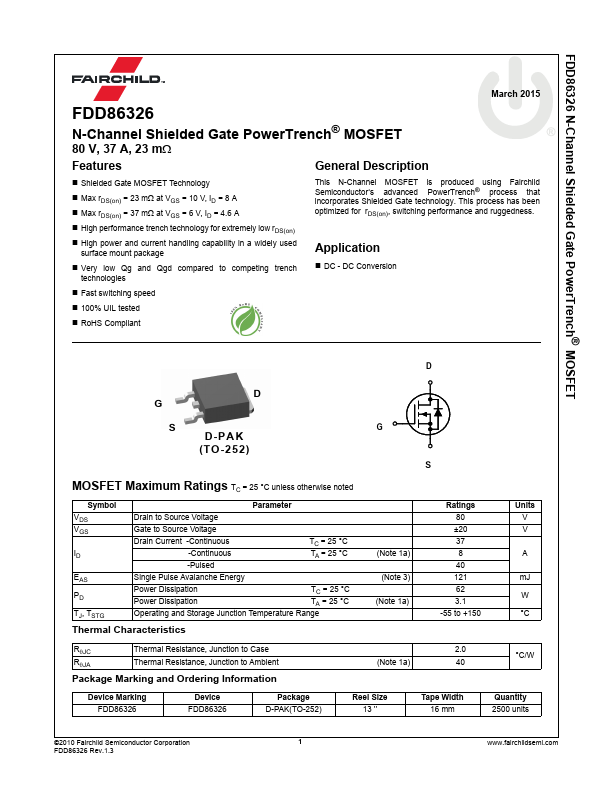
S DT O-P-2A5K2
(T O -25 2)
MOSFET Maximum Ratings TC = 25 °C unless otherwise noted
Symbol VDS VGS
EAS PD TJ, TSTG
Parameter
Drain to Source Voltage
Gate to Source Voltage
Drain Current -Continuous -Continuous -Pulsed
TC = 25 °C TA = 25 °C
Single Pulse Avalanche Energy
Power Dissipation
TC = 25...