FDD8782
Description
This N-Channel MOSFET has been designed specifically to improve the overall efficiency of DC/DC converters using either synchronous or conventional switching PWM controllers. It has been optimized for low gate charge, low rDS(on) and fast switching speed.
Key Features
- Max rDS(on) = 11.0mΩ at VGS = 10V, ID = 35A
- Max rDS(on) = 14.0mΩ at VGS = 4.5V, ID = 35A
- Low gate charge: Qg(10) = 18nC(Typ), VGS = 10V
- Low gate resistance
- Avalanche rated and 100% tested
- RoHS Compliant
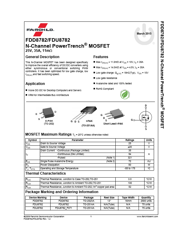
- G DS I-PAK S G (TO-251AA) Short Lead I-PAK MOSFET Maximum Ratings TC = 25°C unless otherwise noted Symbol Parameter VDS Drain to Source Voltage VGS Gate to Source Voltage Drain Current -Continuous (Package Limited) ID -Continuous (Die Limited) -Pulsed