FDMS8050
Overview
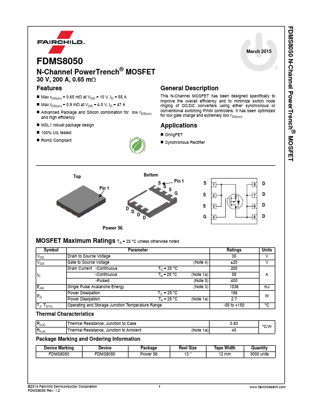
Max rDS(on) = 0.65 mΩ at VGS = 10 V, ID = 55 A Max rDS(on) = 0.9 mΩ at VGS = 4.5 V, ID = 47 A Advanced Package and Silicon combination for low rDS(on) and high efficiency This N-Channel MOSFET has been designed specifically to improve the overall efficiency and to minimize switch node ringing of DC/DC converters using either synchronous or conventional switching PWM controllers. It has been optimized for low gate charge and extremely low rDS(on).