FDP3651U
Features
- RDS(on) = 15 mΩ ( Typ.) @ VGS = 10 V, ID = 80 A
- High Performance Trench Technology for Extremely Low RDS(on)
- Low Miller Charge
- UIS Capability (Single Pulse and Repetitive Pulse)
Applications
- Consumer Appliances
- Synchronous Rectification
- Battery Protection Circuit
- Motor drives and Uninterruptible Power Supplie s
- Micro Solar Inverter
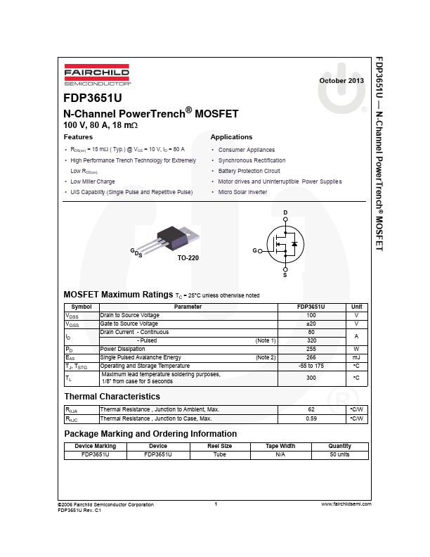
GD S
TO-220
MOSFET Maximum Ratings TC = 25°C unless otherwise noted
Symbol VDSS VGSS ID PD EAS TJ, TSTG TL Parameter Drain to Source Voltage Gate to Source Voltage Drain Current
- Continuous
- Pulsed Power Dissipation Single Pulsed Avalanche Energy Operating and Storage Temperature Maximum lead temperature soldering purposes, 1/8” from case for 5 seconds (Note 2) (Note 1) FDP3651U 100 ±20 80 320 255 266 -55 to 175 300 Unit V V A W m J °C °C
Thermal Characteristics
RθJA RθJC Thermal Resistance , Junction to Ambient, Max. Thermal Resistance , Junction to Case, Max. 62 0.59 °C/W °C/W
Package Marking and Ordering...