Datasheet Details
| Part number | MMBFJ270 |
|---|---|
| Manufacturer | Fairchild ↗ |
| File Size | 46.47 KB |
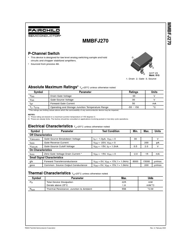
| Description | P-Channel Switch |
| Datasheet |
 MMBFJ270_FairchildSemiconductor.pdf MMBFJ270_FairchildSemiconductor.pdf
|
| Part number | MMBFJ270 |
|---|---|
| Manufacturer | Fairchild ↗ |
| File Size | 46.47 KB |
| Description | P-Channel Switch |
| Datasheet |
MMBFJ270_FairchildSemiconductor.pdf
|
📁 MMBFJ270 Similar Datasheet