Datasheet4U Logo Datasheet4U.com

33889

System Basis Chip

33889 Features

* VDD1: 5.0 V low drop voltage regulator, current limitation, overtemperature detection, monitoring and reset function with total current capability 200 mA

* V2: tracking function of VDD1 regulator; control circuitry for external bipolar ballast transistor for high flexibility in cho

33889 General Description

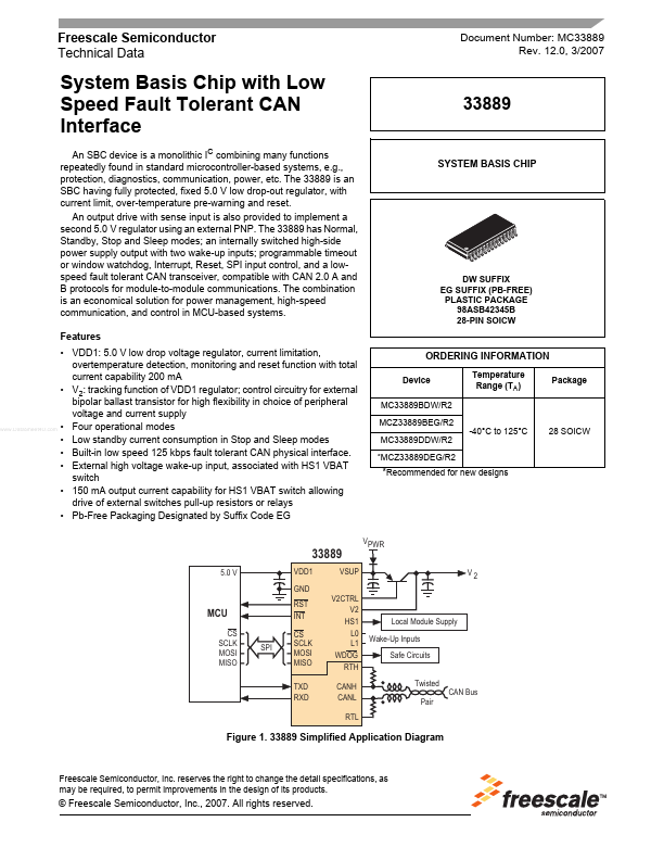
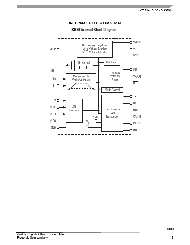
of each pin can be found in the Functional pin description section page 24. Pin 1 2 3 Pin Name RX Pin Function Output Input Power Output Formal Name Receiver Data Transmitter Data Voltage Regulator One Definition CAN bus receive data output pin CAN bus receive data input pin 5.0 V pin is a 2% low.

33889 Datasheet (2.18 MB)

Preview of 33889 PDF

Datasheet Details

Part number:

33889

Manufacturer:

Freescale Semiconductor

File Size:

2.18 MB

Description:

System basis chip.
Freescale Semiconductor Technical Data Document Number: MC33889 Rev. 12.0, 3/2007 System Basis Chip with Low Speed Fault Tolerant CAN Interface An S.

📁 Related Datasheet

33880 Configurable Octal Serial Switch (Freescale Semiconductor)

33882 Six-Output Low-Side Switch (Freescale Semiconductor)

33883 H-Bridge Gate Driver IC (Freescale Semiconductor)

33884 Switch Monitor Interface (Freescale Semiconductor)

33886 5.0A H-Bridge (Freescale Semiconductor)

33887 5.0A H-Bridge with Load Current Feedback (NXP)

33887 5.0 A H-Bridge with Load Current Feedback (Motorola Inc)

33888 Quad High-Side and Octal Low-Side Switch for Automotive (Motorola Inc)

33888A Quad High-Side and Octal Low-Side Switch for Automotive (Motorola Inc)

33889 System basis chip (NXP)

TAGS

33889 System Basis Chip Freescale Semiconductor

Image Gallery

33889 Datasheet Preview Page 2 33889 Datasheet Preview Page 3

33889 Distributor