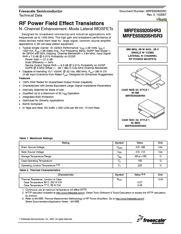
Datasheet4U Logo Datasheet4U.com

MRFE6S9205HR3 - RF Power Field Effect Transistors

Key Features

  • 100% PAR Tested for Guaranteed Output Power Capability.
  • Characterized with Series Equivalent Large - Signal Impedance Parameters.
  • Internally Matched for Ease of Use.
  • Qualified Up to a Maximum of 32 VDD Operation.
  • Integrated ESD Protection.
  • Optimized for Doherty.

📥 Download Datasheet

Full PDF Text Transcription (Reference)

The following content is an automatically extracted verbatim text from the original manufacturer datasheet and is provided for reference purposes only.

View original datasheet text
Freescale Semiconductor Technical Data RF Power Field Effect Transistors N - Channel Enhancement - Mode Lateral MOSFETs Designed for broadband commercial and industrial applications with frequencies up to 1000 MHz. The high gain and broadband performance of these devices make them ideal for large - signal, common - source amplifier applications in 28 volt base station equipment. • Typical Single - Carrier W - CDMA Performance: VDD = 28 Volts, IDQ = 1400 mA, Pout = 58 Watts Avg., Full Frequency Band, 3GPP Test Model 1, 64 DPCH with 50% Clipping, Channel Bandwidth = 3.84 MHz, Input Signal PAR = 7.5 dB @ 0.01% Probability on CCDF. Power Gain — 21.2 dB Drain Efficiency — 34% Device Output Signal PAR — 6.3 dB @ 0.01% Probability on CCDF ACPR @ 5 MHz Offset — - 39.1 dBc in 3.