GS815018AB-357
Key Features
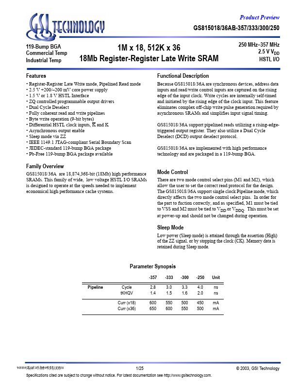
- Register-Register Late Write mode, Pipelined Read mode
- 2.5 V +200/–200 mV core power supply
- 1.5 V or 1.8 V HSTL Interface
- ZQ controlled programmable output drivers
- Dual Cycle Deselect
- Fully coherent read and write pipelines
- Differential HSTL clock inputs, K and K
- Asynchronous output enable
- Sleep mode via ZZ
- IEEE 1149.1 JTAG-compliant Serial Boundary Scan