HM100N06P
Features
:
- Low Intrinsic Capacitances.
- Excellent Switching Characteristics.
- Extended Safe Operating Area.
- Unrivalled Gate Charge :Qg= 72n C (Typ.).
- BVDSS=60V,I D=100A
- RDS(on) : 11mΩ (Max) @VG=10V
- 100% Avalanche Tested
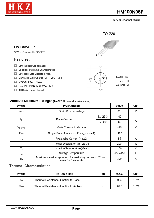
1 23
1.Gate (G) 2.Drain (D) 3.Source (S)
Absolute Maximum Ratings- (Tc=25℃ Unless otherwise noted)
Symbol
PARAMETER
VDSS ID
Drain-Source Voltage Drain Current
TC=25℃ TC=100℃
VGS(TH)
Gate Threshold Voltage
Single Pulse Avalanche Energy (note1)
Avalanche Current (note2)
Power Dissipation (Tc=25℃)
Tj
Junction Temperature(MAX)
Tstg
Storage Temperature
Maximum lead temperature for soldering purpose,1/8” from case for 5 seconds
Thermal Characteristics
Value 60 100 65 ±25 100 85 200 150
-55~+150 300
Symbol RθJC RθJA
PARAMETER Thermal Resistance,Junction to Case Thermal Resistance,Junction to Ambient
Typ.
MAX.
- 0.63
-...