Datasheet Details
- Part number
- CD4081BN, CD4081B
- Manufacturer
- HTC
- File Size
- 157.46 KB
- Datasheet
- CD4081B-HTC.pdf
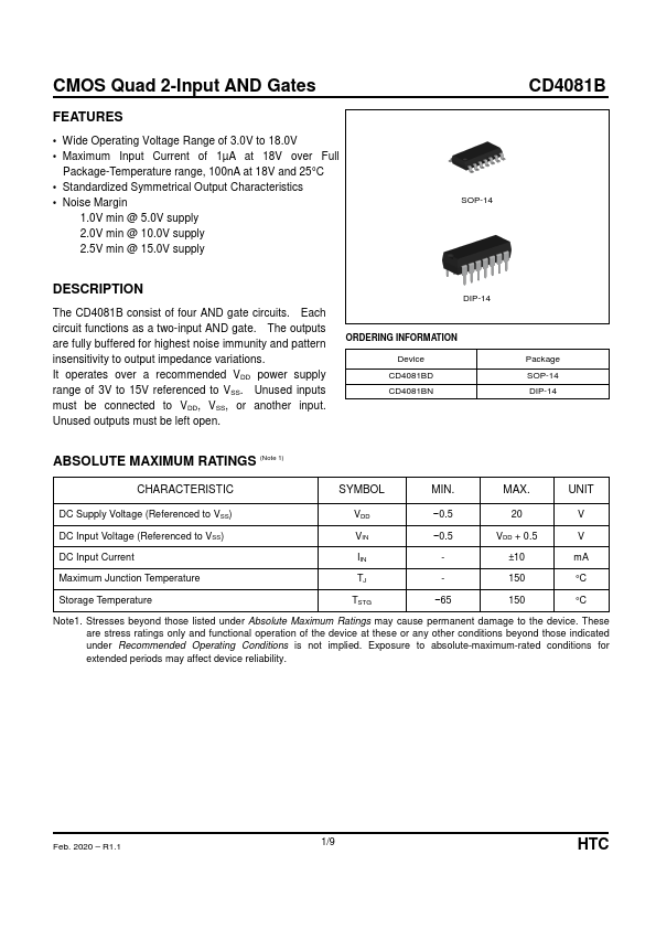
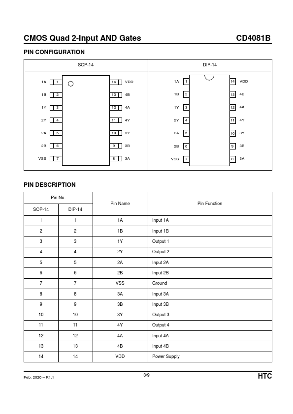
- Description
- CMOS Quad 2-Input AND Gates
- Note
- This datasheet PDF includes multiple part numbers: CD4081BN, CD4081B.
Please refer to the document for exact specifications by model.