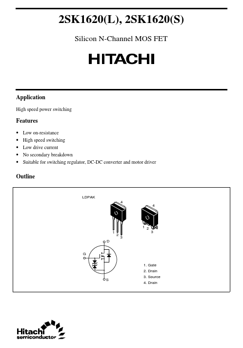
Suitable for switching regulator, DC-DC converter and motor driver
Outline
LDPAK
4
4
123 D
12 3
G S
1. Gate 2. Drain 3. Source 4. Drain
2SK1620(L), 2SK1620(S)
Absolute Maximum Ratings (Ta = 25°C)
Item Drain to source voltage Gate to source voltage Drain current Drain peak current Body to drain diode reverse drain current Channel dissipation Channel temperatu.
Full PDF Text Transcription for 2SK1620L (Reference)
Note: Below is a high-fidelity text extraction (approx. 800 characters) for
2SK1620L. For precise diagrams, and layout, please refer to the original PDF.
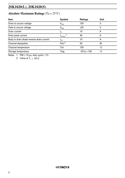
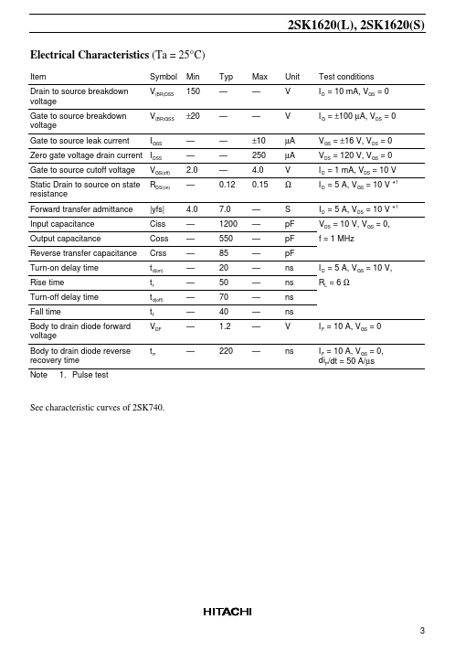
2SK1620(L), 2SK1620(S) Silicon N-Channel MOS FET Application High speed power switching Features • Low on-resistance • High speed switching • Low drive current • No secon...
View more extracted text
ow on-resistance • High speed switching • Low drive current • No secondary breakdown • Suitable for switching regulator, DC-DC converter and motor driver Outline LDPAK 4 4 123 D 12 3 G S 1. Gate 2. Drain 3. Source 4. Drain 2SK1620(L), 2SK1620(S) Absolute Maximum Ratings (Ta = 25°C) Item Drain to source voltage Gate to source voltage Drain current Drain peak current Body to drain diode reverse drain current Channel dissipation Channel temperature Storage temperature Notes 1. PW ≤ 10 µs, duty cycle ≤ 1% 2.