HAT2049T
Features
- -
- - Low on-resistance Capable of 2.5 V gate drive Low drive current High density mounting
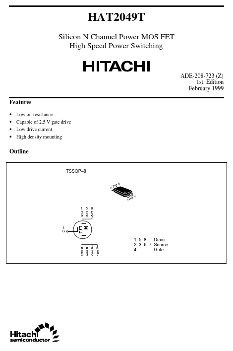
Outline
TSSOP- 8
65 34
12 1 5 8 D D D
4 G
S S S S 2 3 6 7
1, 5, 8 Drain 2, 3, 6, 7 Source 4 Gate
Absolute Maximum Ratings (Ta = 25°C)
Item Drain to source voltage Gate to source voltage Drain current Drain peak current Body-drain diode reverse drain current Channel dissipation Channel temperature Storage temperature Note: Symbol VDSS VGSS ID I D(pulse) I DR Pch Tch Tstg
Note2 Note1
Ratings 30 ± 12 8 64 8 1.3 150
- 55 to + 150
Unit V V A A A W °C °C
1. PW ≤ 10 µs, duty cycle ≤ 1 % 2. When using the glass epoxy board (FR4 40 x 40 x 1.6 mm), PW≤ 10s
Electrical Characteristics (Ta = 25°C)
Item Symbol Min 30 ± 12
- - 0.4
- - 13
- -
- -
- -
- -
- Typ
- -
- -
- 0.013 0.017 20 1430 410 265 23 165 215 185 0.83 30 Max
- - ± 0.1 1 1.4 0.017 0.025
- -
- -
- -
- - 1.08
- Unit V V µA µA V Ω Ω S p F p F p F ns ns ns ns V ns IF = 8 A , VGS = 0 Note3 IF = 8 A, VGS = 0 di F/ dt = 20...