PF0311
Features
- Small package: 30 × 10 × 5.9 mm
- High efficiency: 50% Typ
- Low power control current: 0.5 m A Max
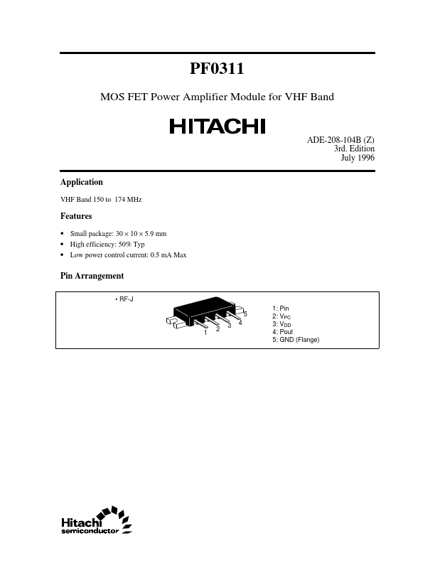
Pin Arrangement
- RF-J 5 1 2 3 4 1: Pin 2: VPC 3: VDD 4: Pout 5: GND (Flange)
Internal Diagram and External Circuit
G GND Pin1 Pin Pin2 VPC Pin3 VDD Pin4 Pout
G GND
Z1
C1
FB1
C3
C4
FB2
C2
Z2
Pin
Pout
C1 = C2 = 0.01 µF (Ceramic chip capacitor) C3 = C4 = 10 µF (Aluminum Electrolyte Capacitor) FB = Ferrite bead BL01RN1-A62-001 (Manufacture: MURATA) or equivalent Z1 = Z2 = 50 Ω (Microstrip line)
Absolute Maximum Ratings (Tc = 25°C)
Item Supply voltage Supply current PC voltage Input power Operating case temperature Storage temperature Symbol VDD I DD VPC Pin Tc (op) Tstg Rating 17 3 7 100
- 30 to +100
- 40 to +110 Unit V A V m W °C °C
Electrical Characteristics (Tc = 25°C)
Item Frequency range Drain cutoff current Total efficiency 2nd harmonic distortion 3rd harmonic distortion 4th harmonic distortion Input VSWR Output power (1) Output...