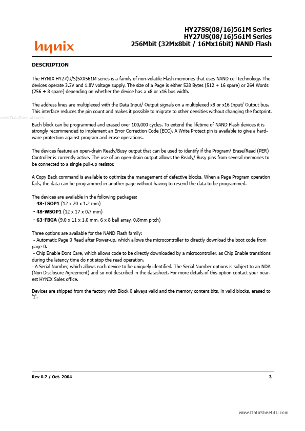
HY27SS16561M - (HY27xSxx561M) 256Mbit (32Mx8bit / 16Mx16bit) NAND Flash
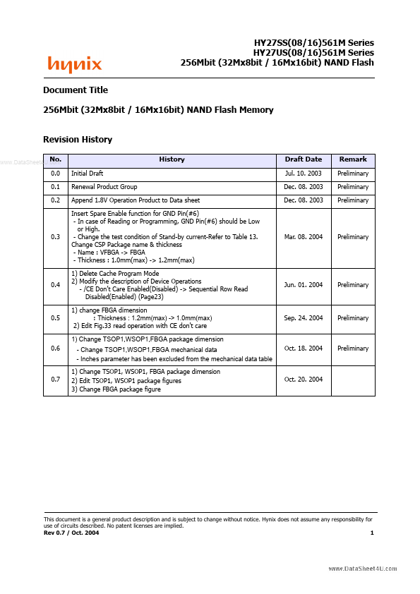
of Device Operations - /CE Don’t Care Enabled(Disabled) -> Sequential Row Read Disabled(Enabled) (Page23) 1) change FBGA dimension : Thickness : 1.2mm(max) -> 1.0mm(max) 2) Edit Fig.33 read operation with CE don't care 1) Change TSOP1,WSOP1,FBGA package dimension 0.6 - Change TSOP1,WSOP1,FBGA mechan
HY27SS(08/16)561M Series HY27US(08/16)561M Series 256Mbit (32Mx8bit / 16Mx16bit) NAND Flash Document Title 256Mbit (32Mx8bit / 16Mx16bit) NAND Flash Memory Revision History No.
www.DataSheet4U.com 0.0 0.1 0.2 Initial Draft Renewal Product Group Append 1.8V Operation Product to Data sheet Insert Spare Enable function for GND Pin(#6) - In case of Reading or Programming, GND Pin(#6) should be Low or High.
- Change the test condition of Stand-by current-Refer to Table 13.
Change CSP Package name & t
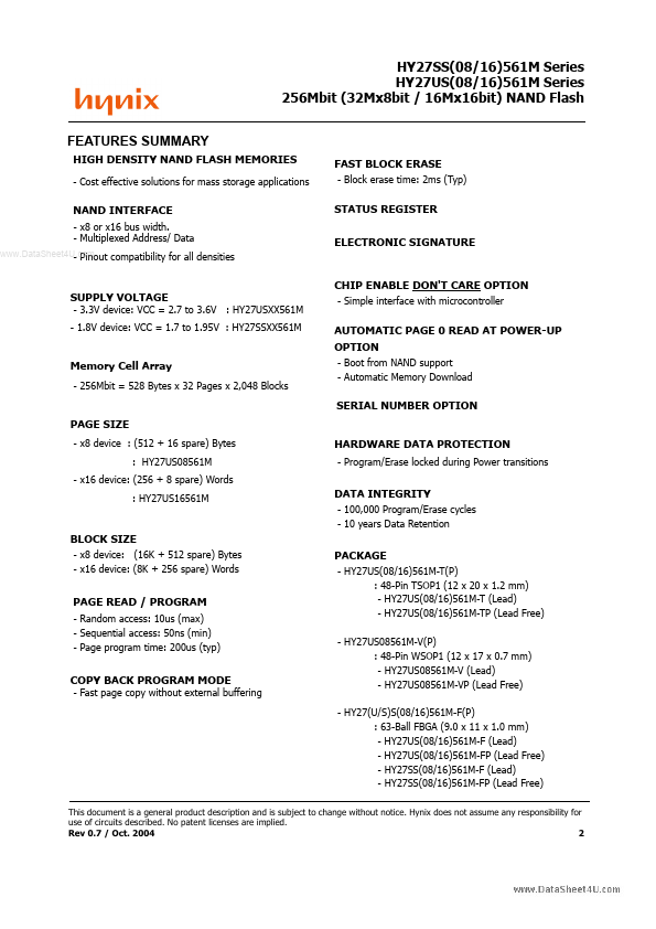
HY27SS16561M Features
* SUMMARY HIGH DENSITY NAND FLASH MEMORIES - Cost effective solutions for mass storage applications FAST BLOCK ERASE - Block erase time: 2ms (Typ) NAND INTERFACE - x8 or x16 bus width. - Multiplexed Address/ Data www.DataSheet4U.com - Pinout compatibility for all densities STATUS REGISTER ELECTRONI