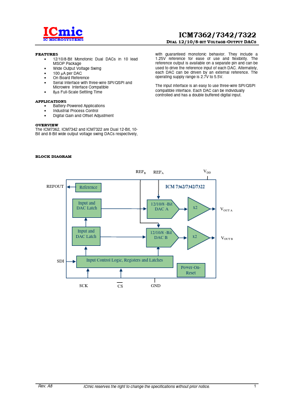
Description
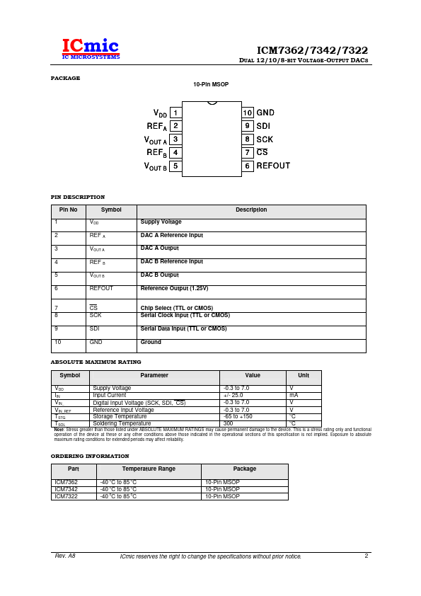
Pin No 1
Symbol VDD
2 REF A
3 VOUT A
4 REF B
5 VOUT B
6 REFOUT
Supply Voltage DAC A Reference Input DAC A Output DAC B Reference Input DAC B Output Reference Output (1.25V)
Description
7 CS 8 SCK
9 SDI
10 GND
Chip Select (TTL or CMOS) Serial Clock Input (TTL or CMOS)
Serial Data Input (TTL or CMOS)
Ground
ABSOLUTE MAXIMUM RATING
Symbol
Parameter
Value
Unit
VDD Supply Voltage
-0.3 to 7.0
V
IIN Input Current
+/- 25.0
mA
VIN_ Digital Input Voltage (SCK, SDI, CS)
-0.3 to 7.0
Features
- 12/10/8-Bit Monotonic Dual DACs in 10 lead MSOP Package.
- Wide Output Voltage Swing.
- 100 µA per DAC.
- On Board Reference.
- Serial Interface with three-wire SPI/QSPI and Microwire Interface Compatible.
- 8µs Full-Scale Settling Time.
 ICM7322-ICmic.pdf