Datasheet Details
| Part number | IDT74LVC16827A |
|---|---|
| Manufacturer | IDT |
| File Size | 102.23 KB |
| Description | 3.3V CMOS 20-BIT BUFFER |
| Datasheet |
 IDT74LVC16827A Datasheet IDT74LVC16827A Datasheet
|
|
|
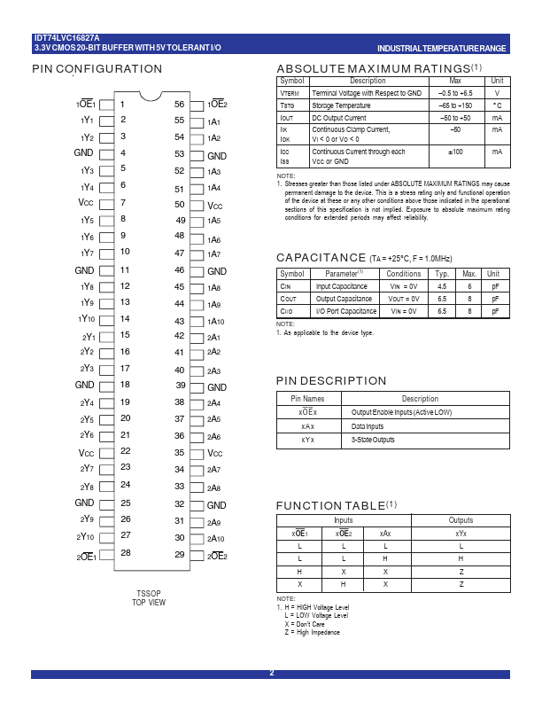
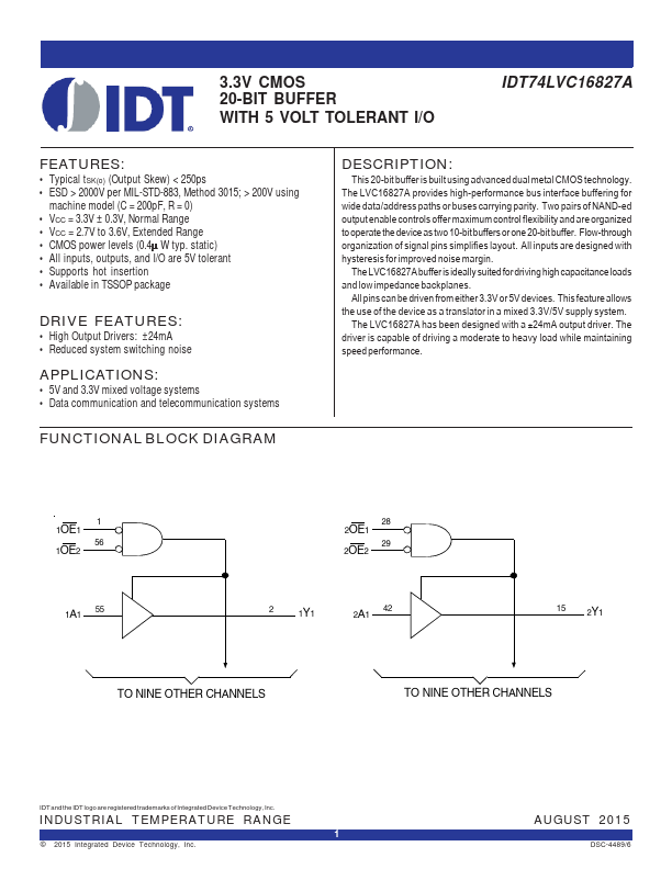
This 20-bit buffer is built using advanced dual metal CMOS technology.
The LVC16827A provides high-performance bus interface buffering for wide data/address paths or buses carrying parity.
| Part number | IDT74LVC16827A |
|---|---|
| Manufacturer | IDT |
| File Size | 102.23 KB |
| Description | 3.3V CMOS 20-BIT BUFFER |
| Datasheet |
IDT74LVC16827A Datasheet
|
|
|
|