IL062
feature high slew rates, low input bias and offset currents, and low offset voltage temperature coefficient.
- -
- -
- -
- - Operation Very low power consumption: 200㎂ Wide mon-mode (up to VCC+) and differential voltage ranges Low input bias and offset currents Output short-circuit protection High input impedance J-FET input stage Internal frequency pensation Latch up free operation High slew rate: 3.5V/s
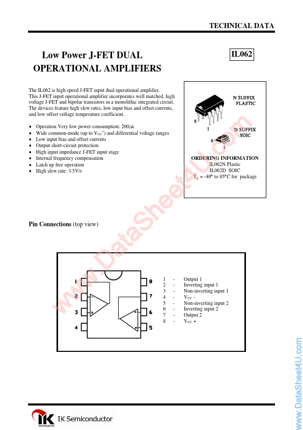
Pin Connections (top view) w w w t a .D
S a e h
1 2 3 4 5 6 7 8
- U 4 t e
ORDERING INFORMATION IL062N Plastic IL062D SOIC TA = -40° to 85°C for package
.c m o
Output 1 Inverting input 1 Non-inverting input 1 VCC Non-inverting input 2 Inverting input 2 Output 2 VCC +
..
SCHEMATIC DIAGRAM
Vcc +
220 Ω Inverting Input Non-inverting Input 64 Ω 45 kΩ Output
270 Ω 3.2 kΩ
1/2 IL062 1/2 TL062C
4.2 kΩ
100 Ω
Vcc
- MAXIMUM RATING
Symbol VCC Vi Vid Ptot Toper Tstg
Notes 1. .
Parameter Supply Voltage
- (note 1) Input Voltage
- (note 3) Differential Input Voltage...