IN74HC74A
TECHNICAL DATA
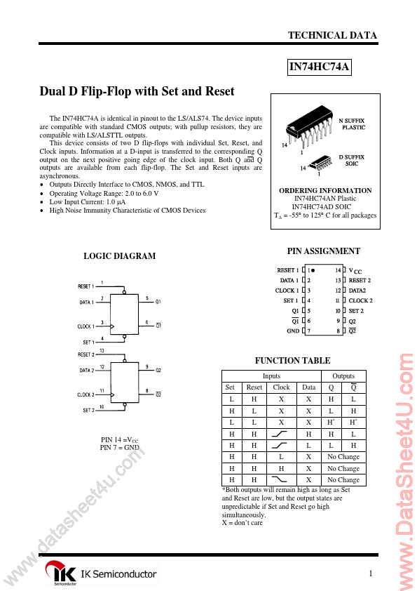
Dual D Flip-Flop with Set and Reset
The IN74HC74A is identical in pinout to the LS/ALS74. The device inputs are patible with standard CMOS outputs; with pullup resistors, they are patible with LS/ALSTTL outputs. This device consists of two D flip-flops with individual Set, Reset, and Clock inputs. Information at a D-input is transferred to the corresponding Q output on the next positive going edge of the clock input. Both Q and Q outputs are available from each flip-flop. The Set and Reset inputs are asynchronous.
- Outputs Directly Interface to CMOS, NMOS, and TTL
- Operating Voltage Range: 2.0 to 6.0 V
- Low Input Current: 1.0 µA
- High Noise Immunity Characteristic of CMOS Devices
ORDERING INFORMATION IN74HC74AN Plastic IN74HC74AD SOIC TA = -55° to 125° C for all packages
LOGIC DIAGRAM
PIN ASSIGNMENT
FUNCTION TABLE
Inputs Set L H L PIN 14 =VCC PIN 7 = GND H H H H Reset H L L H H H H L H Clock X X X Data X X X H L X X Outputs Q H L H
- Q L H H- L...