IW4013B
TECHNICAL DATA
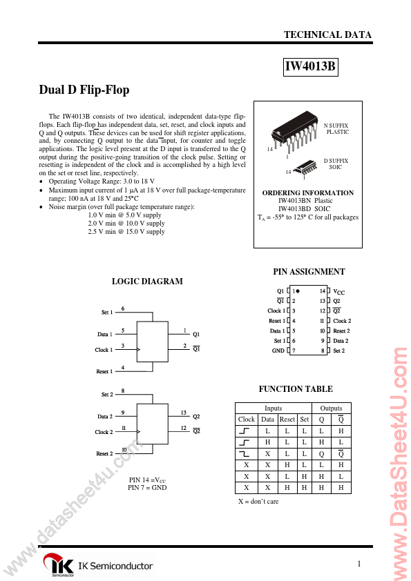
IW4013B Dual D Flip-Flop
The IW4013B consists of two identical, independent data-type flipflops. Each flip-flop has independent data, set, reset, and clock inputs and Q and Q outputs. These devices can be used for shift register applications, and, by connecting Q output to the data input, for counter and toggle applications. The logic level present at the D input is transferred to the Q output during the positive-going transition of the clock pulse. Setting or resetting is independent of the clock and is acplished by a high level on the set or reset line, respectively.
- Operating Voltage Range: 3.0 to 18 V
- Maximum input current of 1 µA at 18 V over full package-temperature range; 100 n A at 18 V and 25°C
- Noise margin (over full package temperature range): 1.0 V min @ 5.0 V supply 2.0 V min @ 10.0 V supply 2.5 V min @ 15.0 V supply
N SUFFIX PLASTIC 14 1 14 1 D SUFFIX SOIC
ORDERING INFORMATION IW4013BN Plastic IW4013BD SOIC TA = -55° to 125° C for all packages
PIN...