IW4027B
features independent Set, Reset, and Clock inputs. Data is accepted when the Clock is LOW and transferred to the output on the positive-going edge of the Clock. The active HIGH asynchronous Reset and Set are independent and override the J, K, or Clock inputs. The outputs are buffered for best system performance.
- Operating Voltage Range: 3.0 to 18 V
- Maximum input current of 1 µA at 18 V over full package-temperature range; 100 n A at 18 V and 25°C
- Noise margin (over full package temperature range): 1.0 V min @ 5.0 V supply 2.0 V min @ 10.0 V supply 2.5 V min @ 15.0 V supply
ORDERING INFORMATION IW4027BN Plastic IW4027BD SOIC TA = -55° to 125° C for all packages
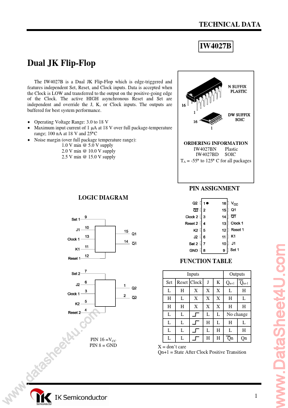
PIN ASSIGNMENT LOGIC DIAGRAM
FUNCTION TABLE
Inputs Set Reset Clock L H H H L H L L L L X X X J X X X L H L H K X X X L L H H Outputs Qn+1 L H H H L Qn Qn+1 H L H L H Qn w w w
.d h s a t a ee
. u t4 m o c
PIN 16 =VCC PIN 8 = GND
No change
X = don’t care Qn+1 = State After Clock Positive...