IW4050B
feature logic-level conversion using only one supply (voltage (VCC). The input-signal high level (VIH) can exceed the VCC supply voltage when these devices are used for logic-level conversions. These devices are intended for use as CMOS to DTL/TTL converters.
- Operating Voltage Range: 3.0 to 18 V
- Maximum input current of 1 µA at 18 V over full package-temperature range; 100 n A at 18 V and 25°C
- Noise margin (over full package temperature range): 1.0 V min @ 5.0 V supply 2.0 V min @ 10.0 V supply 2.5 V min @ 15.0 V supply
- High-to-low level conversion
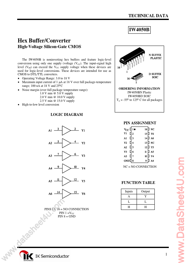
ORDERING INFORMATION IW4050BN Plastic IW4050BD SOIC TA = -55° to 125° C for all packages
LOGIC DIAGRAM PIN ASSIGNMENT
NC = NO CONNECTION
FUNCTION TABLE
Inputs A Output Y L H w w w
.d e e h s a t a
. u t4
PINS 13, 16 = NO CONNECTION PIN 1 =VCC PIN 8 = GND m o c
..
MAXIMUM RATINGS-
Symbol VCC VIN VOUT IIN PD PD Tstg TL
- Parameter DC Supply Voltage (Referenced to GND) DC Input Voltage (Referenced to GND)...