IW4069UB
TECHNICAL DATA
Hex Inverter
High-Voltage Silicon-Gate CMOS
The IW4069UB types consist of six inverter circuits. These devices are intended for all general-purpose inverter applications where the mediumpower TTL-drive and logic-level-conversion capabilities of circuits such as the IW4049UB Hex Inverter/Buffers are not required. Each of the six inverters is a single stage
- Operating Voltage Range: 3.0 to 18 V
- Maximum input current of 1 µA at 18 V over full package-temperature range; 100 n A at 18 V and 25°C
- Noise margin (over full package temperature range): 0.5 V min @ 5.0 V supply 1.0 V min @ 10.0 V supply 1.5 V min @ 15.0 V supply
ORDERING INFORMATION IW4069UBN Plastic IW4069UBD SOIC TA = -55° to 125° C for all packages
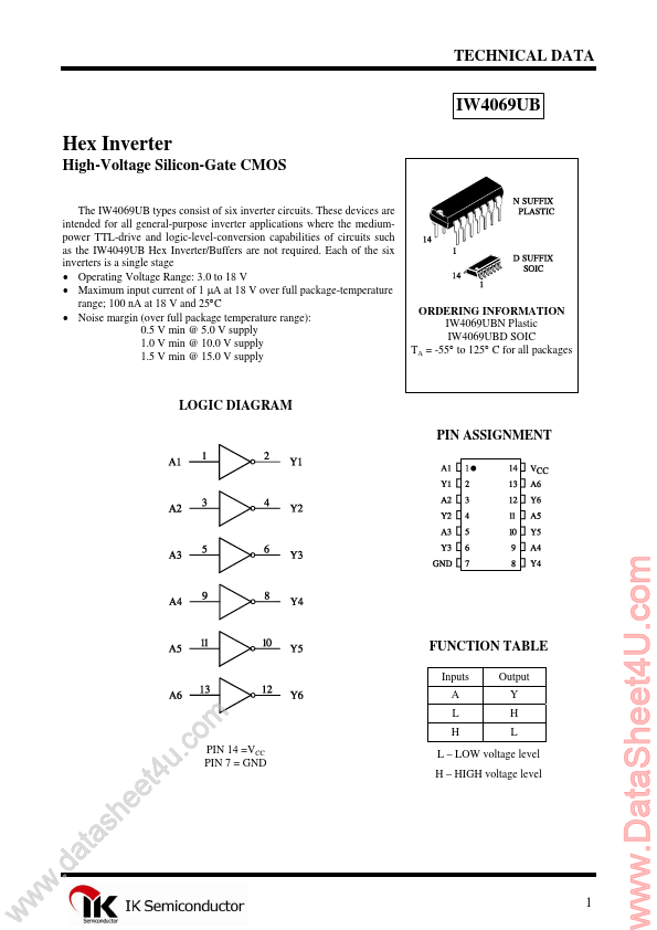
LOGIC DIAGRAM PIN ASSIGNMENT
FUNCTION TABLE
Inputs A Output Y H L w w w
.d e e h s a t a
. u t4 m o c
PIN 14 =VCC PIN 7 = GND
- LOW voltage level H
- HIGH voltage level
..
MAXIMUM RATINGS-
Symbol VCC VIN IIN PD Ptot...