IW4502B
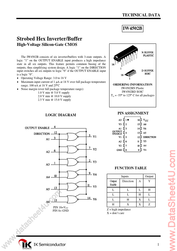
feature permits mon busing of the outputs, thus simplifying system design. A logic “1” on the DIRECTION input switches all six outputs to logic “0” if the OUTPUT ENABLE input is a logic “0”.
- Operating Voltage Range: 3.0 to 18 V
- Maximum input current of 1 µA at 18 V over full package-temperature range; 100 n A at 18 V and 25°C
- Noise margin (over full package temperature range): 1.0 V min @ 5.0 V supply 2.0 V min @ 10.0 V supply 2.5 V min @ 15.0 V supply
ORDERING INFORMATION IW4502BN Plastic IW4502BD SOIC TA = -55° to 125° C for all packages
LOGIC DIAGRAM
PIN ASSIGNMENT
FUNCTION TABLE
Inputs Output Enable Direction L L H X A L H X X Output Y H L L Z w w w
.d e e h s a t a
. u t4 m o c
PIN 16=VCC PIN 8= GND
Z = high impedance X = don’t care
..
MAXIMUM RATINGS-
Symbol VCC VIN VOUT IIN PD PD Tstg TL
- Parameter DC Supply Voltage (Referenced to GND) DC Input Voltage (Referenced to GND) DC Output Voltage (Referenced to GND) DC Input Current, per Pin...