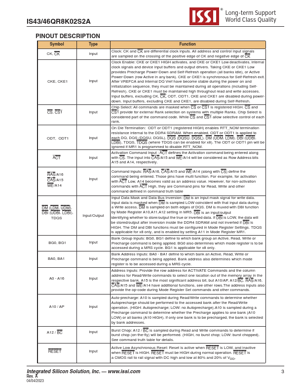
Description
Symbol
Type
CK, CK
Input
CKE, CKE1
Input
CS, CS1
Input
ODT, ODT1
ACT
RAS/A16 CAS/A15 WE/A14
Input Input Input
DM (LDM, UDM), DBI (UDBI, LDBI),
TDQS
Input/Output
BG0, BG1 BA0, BA1 A0 - A16
Input Input Input
A10 / AP A12 / BC RESET
Input Input Input
Function
Clock: CK and CK are differential clock inputs.All address and control input signals are sampled on the crossing of the positive edge of CK and negative edge of CK
Clock Enable: CKE or CKE1 HIGH activates, and CKE or CKE1 Low
Features
- Dual Rank: Each rank has its own CS, ODT, and CKE.
- Standard Voltage : VDD = VDDQ = 1.2V, VPP=2.5V.
- High speed data transfer rates with system frequency
up to 2400 Mbps.
- Data Integrity
- Auto Self Refresh (ASR) by DRAM built-in TS - Auto Refresh and Self Refresh Modes.
- DRAM access bandwidth - Separated IO gating structures by Bank Groups - Self Refresh Abort - Fine Granularity Refresh.
- Signal Synchronization - Write Leveling via MR settings -.
 IS46QR8K02S2A-ISSI.pdf