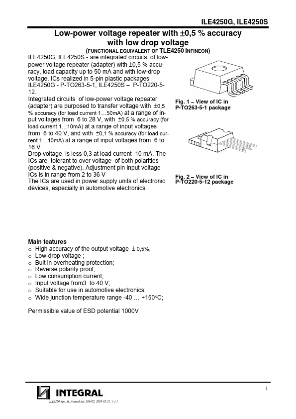
Description
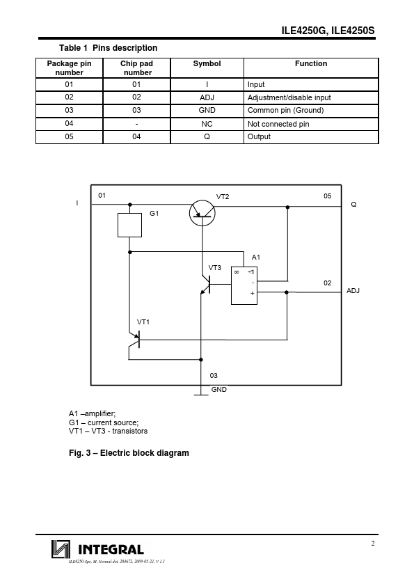
Package pin number 01 02 03 04 05
Chip pad number
01 02 03 04
ILE4250G, ILE4250S
Symbol
I ADJ GND NC
Q
Function
Input Adjustment/disable input Common pin (Ground) Not connected pin Output
01 I
G1
VT1
VT2
A1 VT3 ∞
+
Δ
A1
amplifier; G1
current source; VT1
VT3 - transistors
Fig.3
Electric block diagram
03 GND
05 Q
02 ADJ
ILE4250-Spe, M, Normal.dot, 284672, 2009-05-21, V 1.1
2
Table 2 Absolute Maximum Ratings
Symbol Parameters
ТJ Junction tempe
Features
- o High accuracy of the output voltage ± 0,5%; o Low-drop voltage ; o Buit in overheating protection; o Reverse polarity proof; o Low consumption current; o Input voltage from3 to 40 V; o Suitable for use in automotive electronics; o Wide junction temperature range -40 … +150°C;
Permissible value of ESD potential 1000V
ILE4250-Spe, M, Normal. dot, 284672, 2009-05-21, V 1.1
1
Table 1 Pins.
 ILE4250G-Integral.pdf