S9013LT1
FEATURES
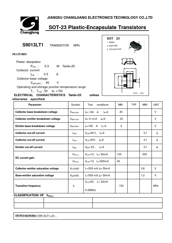
1. BASE
TRANSISTOR£¨NPN £©
2. EMITTER 3. COLLECTOR
Power dissipation PCM : 0.3 W£¨ Tamb=25¡æ£© Collector current ICM : 0.5 A Collector-base voltage V(BR)CBO : 40 V Operating and storage junction temperature range T J £¬ T stg: -55¡æto +150 ELECTRICAL CHARACTERISTICS£¨ Tamb=25¡æ otherwise specified£©
Parameter Collector-base breakdown voltage Collector-emitter breakdown voltage Emitter-base breakdown voltage Collector cut-off current Collector cut-off current Emitter cut-off current Symbol V(BR)CBO V(BR)CEO V(BR)EBO ICBO ICEO IEBO HFE(1) DC current gain HFE(2) Collector-emitter saturation voltage Base-emitter saturation voltage VCE(sat) VBE(sat) unless
Test conditions MIN 40 25 5
Unit : mm
UNIT V V V
Ic= 100¦Ì A£¬ IE=0 Ic= 0.1m A£¬IB=0 IE=100¦Ì A£¬IC=0 VCB=40 V , IE=0 VCE=20V , IB=0 VEB= 5V , IC=0
0.1 0.1 0.1 120 40 0.6 1.2 350
¦Ì A ¦Ì A ¦Ì A
VCE=1V, IC= 50m A VCE=1V, IC=500m A IC=500 m A, IB= 50m A IC=500 m A, IB= 50m A VCE=6V, I C= 20m A
Transition...