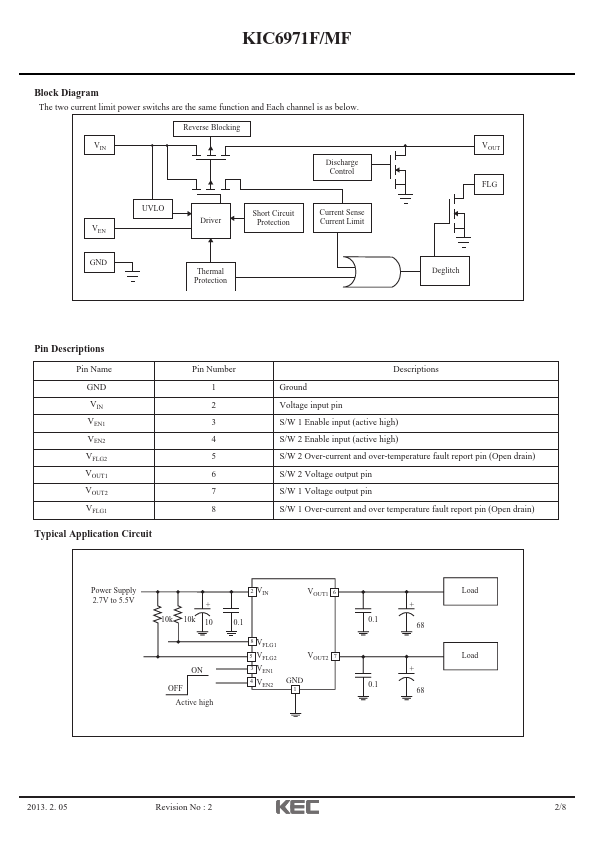
Description
Pin Name GND VIN VEN1 VEN2 VFLG2 VOUT1 VOUT2 VFLG1
Typical Application Circuit
Pin Number 1 2 3 4 5 6 7 8
Descriptions Ground Voltage input pin S/W 1 Enable input (active high) S/W 2 Enable input (active high) S/W 2 Over-current and over-temperature fault report pin (Open drain) S/W 2 Voltage output pin S/W 1 Voltage output pin S/W 1 Over-current and over temperature fault report pin (Open drain)
Power Supply 2.7V to 5.5V
2 VIN
VOUT1 6
+
+
10k 10k 10
0.1
0.1 68
ON
OFF Active high
8
Features
- Single USB Port Power Switches with discharge Operating input voltage range 2.7V to 5.5V Up to 1.5A Maximum Load Current Internal Short Circuit Current Limiting(2.1A) Reverse Current Blocking Fault report with blanking time(7ms) 90m Power MOSFET
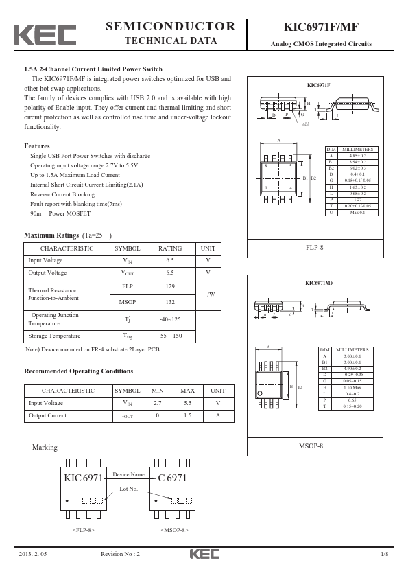
Maximum Ratings (Ta=25 ).
 KIC6971F-KEC.pdf