SY100EL33L
FEATURES s s s s s s 3.3V and 5V power supply options 650ps propagation delay 4.0GHz toggle frequency High bandwidth output transistions Internal 75KΩ input pull-down resistors Available in 8-pin SOIC package
DESCRIPTION
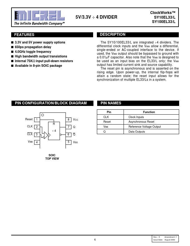
The SY10/100EL33/L are integrated ÷ 4 dividers. The differential clock inputs and the VBB allow a differential, single-ended or AC-coupled interface to the device. If used, the VBB output should be bypassed to ground with a 0.01µF capacitor. Also note that the VBB is designed to be used as an input bias on the EL33/L only; the VBB output has limited current sink and source capability. The reset pin is asynchronous and is asserted on the rising edge. Upon power-up, the internal flip-flops will attain a random state; the reset input allows for the synchronization of multiple EL33/Ls in a system.
PIN CONFIGURATION/BLOCK DIAGRAM
PIN NAMES
Pin Function Clock Inputs Asynchronous Reset Reference Voltage Output Data Outputs
Reset CLK CLK VBB
1 R 2 ÷4 3 4
8 7 6...