PL502-30
DESCRIPTION
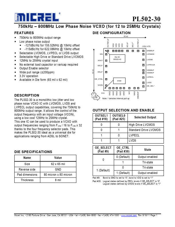
The PL502-30 is a monolithic low jitter and low phase noise VCXO IC with LVCMOS, LVDS and LVPECL output capabilities, covering the 750k Hz to 800MHz output range. It allows the control of the output frequency with an input voltage (VCON), using a low cost 12MHz to 25MHz crystal. This one IC can be used to produce a VCXO with output frequencies ranging from FXIN / 16 to FXIN x 32 thanks to the four frequency selector pads. This makes the PL502-30 ideal as a universal die for applications ranging from ADSL to SONET.
(0,0)
Note: ^ denotes internal pull up
OUTPUT SELECTION AND ENABLE
OUTSEL1 OUTSEL0 (Pad #18) (Pad #25)
Selected Output
0 0 High Drive LVCMOS
0 1 Standard Drive LVCMOS
1 0 LVPECL
1 1 LVDS
DIE SPECIFICATIONS
Name
Value
Size Reverse side Pad dimensions
Thickness
62 x 65 mil GND
80 micron x 80 micron 8 mil
OE_SELECT OE_CTRL
(Pad #9)
(Pad #30)
State
0 (Default)
Output enabled
1 Tri-state
1 (Default)
0 1 (Default)
Tri-state Output...