dsPIC33F - (dsPIC24H / dsPIC33F) Flash Programming Specification
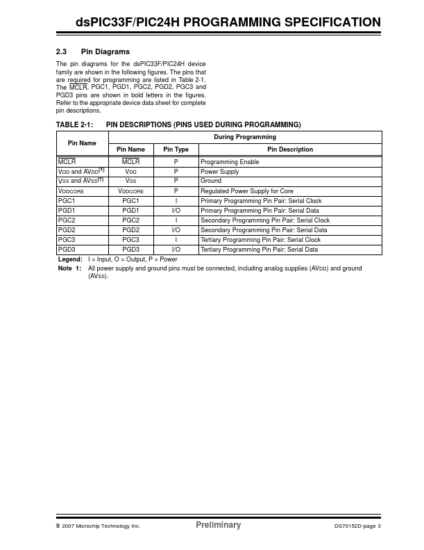
. TABLE 2-1: Pin Name PIN DESCRIPTIONS (PINS USED DURING PROGRAMMING) During Programming Pin Name Pin Type P P P P I I/O I I/O I I/O Programming Enable Power Supply Ground Regulated Power Supply for Core Primary Programming Pin Pair: Serial Clock Primary Programming Pin Pair: Serial Data Secondary.
www.DataSheet4U.com dsPIC33F/PIC24H dsPIC33F/PIC24H Flash Programming Specification 1.0 DEVICE OVERVIEW PIC24HJ128GP306 PIC24HJ128GP310 PIC24HJ128GP506 PIC24HJ128GP510 PIC24HJ256GP206 PIC24HJ256GP210 PIC24HJ256GP610 dsPIC33FJ12GP201 dsPIC33FJ12GP202 dsPIC33FJ12MC201 dsPIC33FJ12MC202 PIC24HJ12GP201 PIC24HJ12GP202 This document defines the programming specification for.
dsPIC33F Features
* PROGRAMMING SPECIFICATION
Pin Diagrams (Continued)
64-Pin TQFP
CSDO/RG13 CSDI/RG12 CSCK/RG14 C2RX/RG0 C2TX/RG1 C1TX/RF1 C1RX/RF0 VDD VDDCORE OC8/CN16/RD7 OC7/CN15/RD6 OC6/IC6/CN14/RD5 OC5/IC5/CN13/RD4 OC4/RD3 OC3/RD2 OC2/RD1 64 63 62 61 60 59 58 57 56 55 5