PC33889DW
PC33889DW is System Basis Chip Lite with Low Speed Fault Tolerant CAN Interface manufactured by Motorola Semiconductor.
features
:
- Vdd1: 5V Low drop voltage regulator, current limitation, over temperature detection, monitoring and reset function. Total current capability 200m A.
- V2: Tracking function of Vdd1 regulator. Control circuitry for external bipolar ballast transistor for high flexibility in choice of peripheral voltage and current supply.
- Four operational modes: normal, stand-by, stop and sleep modes.
- Low stand-by current consumption in stop and sleep modes
- Built in Low speed 125KBaud fault tolerant CAN physical interface, patible with Motorola MC33388.
- External high voltage wake-up input, associated with HS1 Vbat switch
- 150m A output current capability for HS1 Vbat switch allowing drive of external switches pull up resistors or relays
- Vsup monitoring and failure detection
- DC Operating voltage from 5 to 27V
- 40V maximum transient voltage
- Programmable software time out and window watchdog
- Separate outputs for Watchdog time out signal (WDOGB) and Reset (Reset).
- Wake up capabilities: wake up input, programmable cyclic sense, forced wake up, CAN interface, SPI (CSB pin) and stop mode over current.
- Interface with MCU through 4 Mhz SPI.
- SO28WB package with thermal enhanced lead frame.
PC33889
PASS3
System Basis Chip Lite
SILICON MONOLITHIC INTEGRATED CIRCUIT
Freescale Semiconductor, Inc...
DW SUFFIX
PLASTIC PACKAGE CASE 751F SO-28
PIN CONNECTIONS
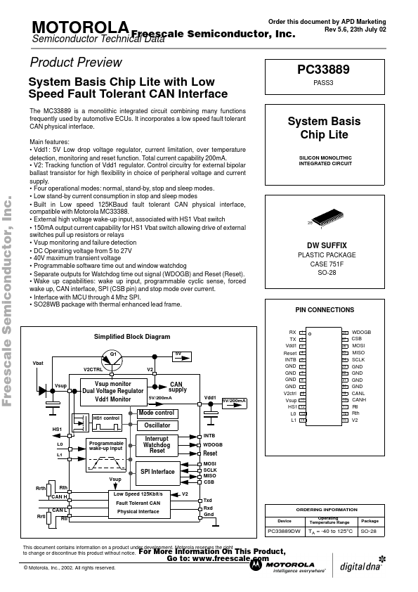
Simplified Block Diagram
Q1 Vbat V2CTRL Vsup V2
5V
Vsup monitor CAN supply Dual Voltage Regulator 5V/200m A Vdd1 Monitor Mode control
HS1 control
Vdd1
5V/200m A
RX TX Vdd1 Reset INTB GND GND GND GND V2ctrl Vsup HS1 L0 L1
1 2 3 4 5 6 7 8 9 10 11 12 13 14
28 27 26 25 24 23 22 21 20 19 18 17 16 15
WDOGB CSB MOSI MISO SCLK GND GND GND GND CANL CANH Rtl Rth V2
HS1
L0 L1
Oscillator
Programmable wake-up...