Description
of Changes
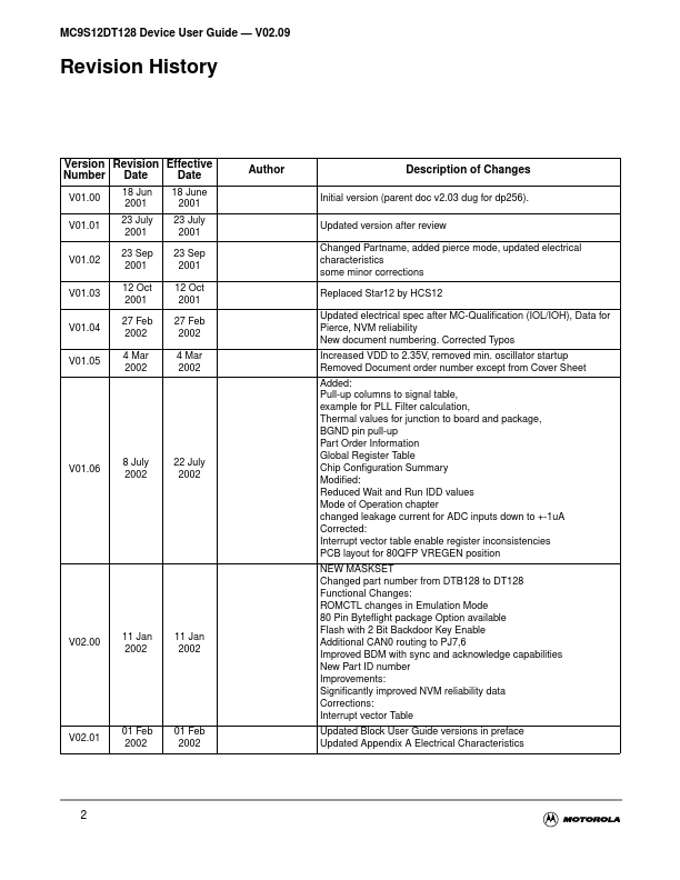
Initial version (parent doc v2.03 dug for dp256).Updated version after review Changed Partname, added pierce mode, updated electrical characteristics some minor corrections Replaced Star12 by HCS12 Updated electrical spec after MC-Qualification (IOL/IOH), Data for Pierce, NVM reliability New document numbering.Corrected Typos Increased VDD to 2.35V, removed min.oscillator startup Removed Document order number except from Cover Sheet Added: Pull-up columns to signal table, example fo
Features
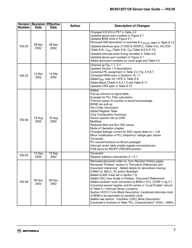
- Corrected KWP5 pin name in Fig 2-1 112LQFP pin assignments Corrected pull resistor CTRL/reset states for PE7 and PE4-PE0 in Table 2.1 “Signal Properties” Mentioned “S12LRAE” bootloader in Flash section 17 Corrected footnote on clamp of TEST pin under Table A-1 “Absolute Maximum Ratings” Corrected minimum bus frequency to 0.25MHz in Table A-4 “Operating Conditions” Replaced “burst programming” by “row programming” in A.3 “NVM, Flash and EEPROM” Corrected blank check time for EEPROM in Table A-11.
 MC9S12DJ128 Datasheet