Description
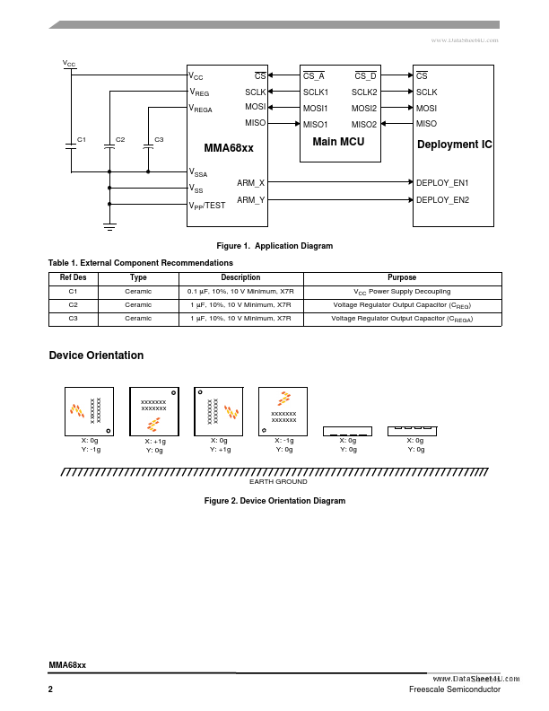
0.1 μF, 10%, 10 V Minimum, X7R 1 μF, 10%, 10 V Minimum, X7R 1 μF, 10%, 10 V Minimum, X7R Purpose VCC Power Supply Decoupling Voltage Regulator Output Capacitor (CREG) Voltage Regulator Output Capacitor (CREGA)
Device Orientation
xxxxxxx xxxxxxx
X: 0g Y: -1g
MMA68xx 2 Sensors Freescale Semiconductor
xxxxxxx xxxxxxx X: +1g Y: 0g
Figure 2. Device Orientation Diagram
xxxxxxx xxxxxxx X: 0g Y: +1g
xxxxxxx xxxxxxx X: -1g Y: 0g X: 0g Y: 0g X: 0g Y: 0g
EARTH GROUND
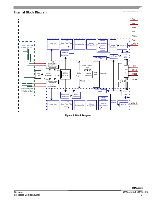
Internal Block Diagram
www.D
Features
- ±20g to ±120 g full-scale range, independently specified for each axis 3.3 V or 5 V single supply operation SPI-compatible serial interface 10-bit digital signed or unsigned SPI data output Independent programmable arming functions for each axis Twelve low-pass filter options, ranging from 50 Hz to 1000 Hz Optional offset cancellation with > 6s averaging period and < 0.25 LSB/s slew rate Pb-Free 16-Pin QFN-6x6 Packag.
 MMA6823QR2 Datasheet