Datasheet4U Logo Datasheet4U.com

M2N2G64TU8HG4B, M2N1G64TUH8G5F Datasheet - Nanya

M2N2G64TU8HG4B, M2N1G64TUH8G5F, Unbuffered DDR2 SO-DIMM

M2N1G64TUH8G5F / M2S1G64TUH8G4F / M2N2G64TU8HG5B / M2N2G64TU8HG4B 1GB: 128M x 64 / 2GB: 256M x 64 PC2-5300 / PC2-6400 Unbuffered DDR2 SO-DIMM Based on.
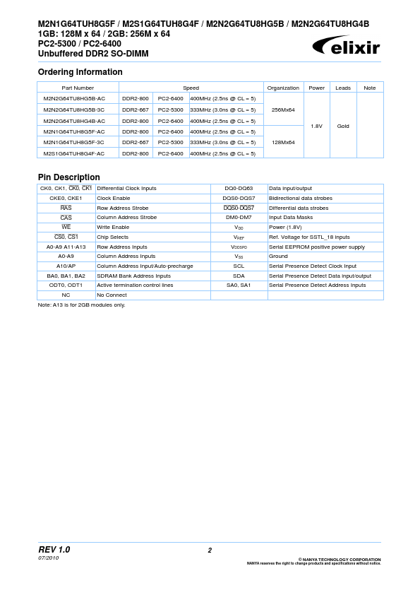
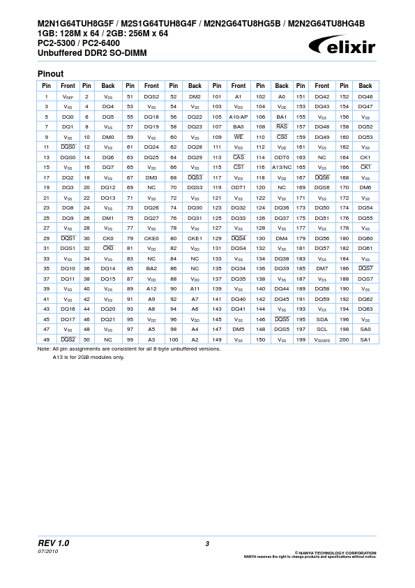
M2N1G64TUH8G5F / M2S1G64TUH8G4F / M2N2G64TU8HG5B / M2N2G64TU8HG4B are unbuffered 200-Pin Double Data Rate 2 (DDR2) Synchronous DRAM Small Outline Dual.
 datasheet Preview Page 1 from Datasheet4u.com

M2N1G64TUH8G5F-Nanya.pdf

This datasheet PDF includes multiple part numbers: M2N2G64TU8HG4B, M2N1G64TUH8G5F. Please refer to the document for exact specifications by model.

Datasheet Details

Part number:

M2N2G64TU8HG4B, M2N1G64TUH8G5F

Manufacturer:

Nanya

File Size:

364.08 KB

Description:

Unbuffered DDR2 SO-DIMM

Note:

This datasheet PDF includes multiple part numbers: M2N2G64TU8HG4B, M2N1G64TUH8G5F.
Please refer to the document for exact specifications by model.

Features

* Performance: Speed Sort DIMM CAS Latency fck
* Clock Freqency tck
* Clock Cycle Data Transfer Speed PC2-5300 -3C 5 333 3 667 PC2-6400 -AC 5 400 2.5 800 MHz ns Mbps
* Automatic and controlled precharge commands
* Programmable Operation: - DIMM  Latency: 3,

Applications

* Inputs and outputs are SSTL-18 compatible
* VDD = VDDQ = 1.8V ± 0.1V
* SDRAMs have 8 internal banks for concurrent operation
* Differential clock inputs
* Data is read or written on both clock edges
* DRAM DLL aligns DQ and DQS transitions with cloc

M2N2G64TU8HG4B Distributors

📁 Related Datasheet

📌 All Tags

Nanya M2N2G64TU8HG4B-like datasheet