Description
This device contains two independent positive-edge-triggered D flip-flops with complementary outputs The information on the D input is accepted by the flip-flops on the positive going edge of the clock pulse The triggering occurs at a voltage level and is not directly related to the transition time of the rising edge of the clock The data on the D input may be changed while the clock is low or high without affecting the outputs as long as the data setup and hold times are not violated A low logi
Features
- Y
Alternate Military Aerospace device (5474) is available Contact a National Semiconductor Sales Office Distributor for specifications
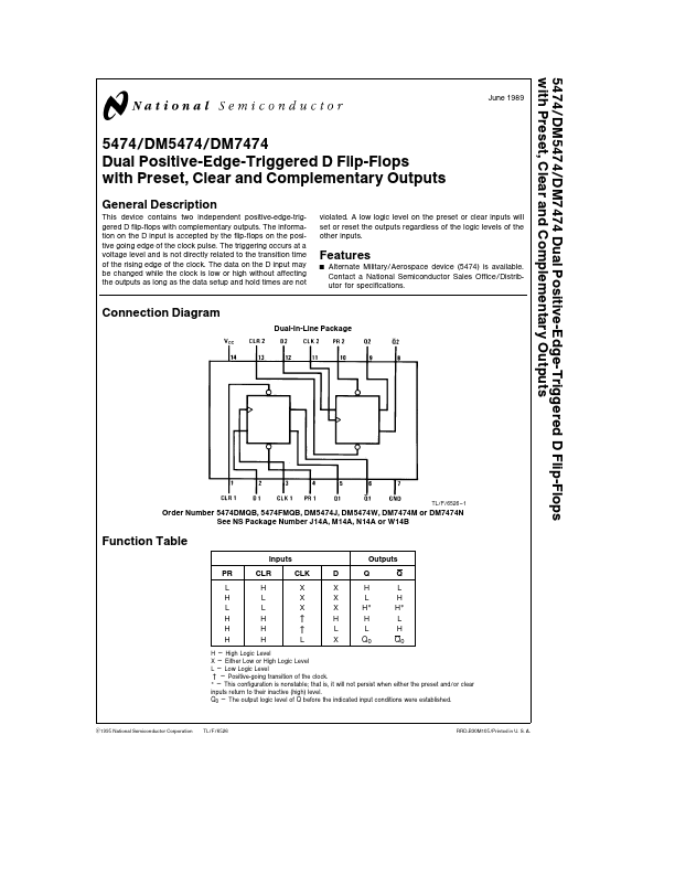
Connection Diagram
Dual-In-Line Package
TL F 6526.
- 1
Order Number 5474DMQB 5474FMQB DM5474J DM5474W DM7474M or DM7474N See NS Package Number J14A M14A N14A or W14B
Function Table
Inputs PR L H L H H H CLR H L L H H H CLK X X X D X X X H L X Outputs Q H L H H L Q0 Q L H H L H Q0
u u
L
H e High Logic Level X e Either Low or High Logic Level L e Low.
 5474_NationalSemiconductor.pdf