Datasheet Details
| Part number | LF198 |
|---|---|
| Manufacturer | National Semiconductor (now Texas Instruments) |
| File Size | 508.90 KB |
| Description | Monolithic Sample-and-Hold Circuits |
| Datasheet |
 LF198 Datasheet LF198 Datasheet
|
|
|
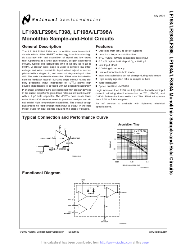
The LF198/LF298/LF398 are monolithic sample-and-hold circuits which utilize BI-FET technology to obtain ultra-high dc accuracy with fast acquisition of signal and low droop rate.
Operating as a unity gain follower, dc gain accuracy is 0.002% typical and acquisition time is as low as 6 µs to 0.01%.
| Part number | LF198 |
|---|---|
| Manufacturer | National Semiconductor (now Texas Instruments) |
| File Size | 508.90 KB |
| Description | Monolithic Sample-and-Hold Circuits |
| Datasheet |
LF198 Datasheet
|
|
|
|